Enhanced charge device model clamp

a charge device and model clamp technology, applied in the field of semiconductor circuits for electrostatic discharge protection in semiconductors, can solve the problems of increasing the vulnerability of high-scaled devices to esd and increasing the risk of damag

Inactive Publication Date: 2015-05-12
GLOBALFOUNDRIES INC
View PDF9 Cites 3 Cited by
  • Summary
  • Abstract
  • Description
  • Claims
  • Application Information

AI Technical Summary

Problems solved by technology

These highly scaled-down devices, however, have been found to be increasingly vulnerable to ESD.
Due to the continuing trend towards miniaturization of electronic devices, smaller critical dimensions and thinner dielectric layers are being used, which are more prone to damage from ESD events.

Method used


Image

  • Enhanced charge device model clamp
  • Enhanced charge device model clamp
  • Enhanced charge device model clamp

Examples


Embodiment Construction

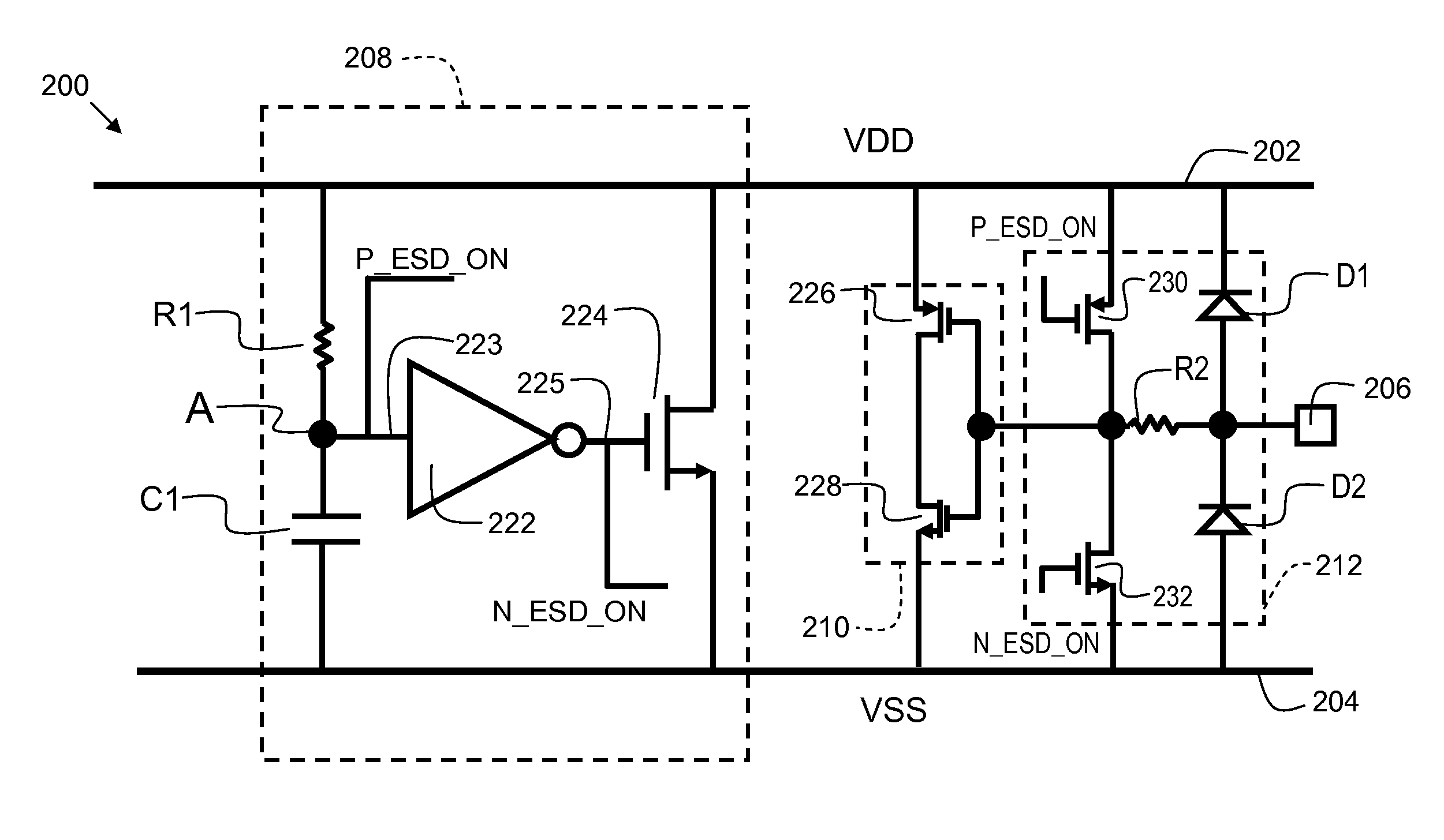
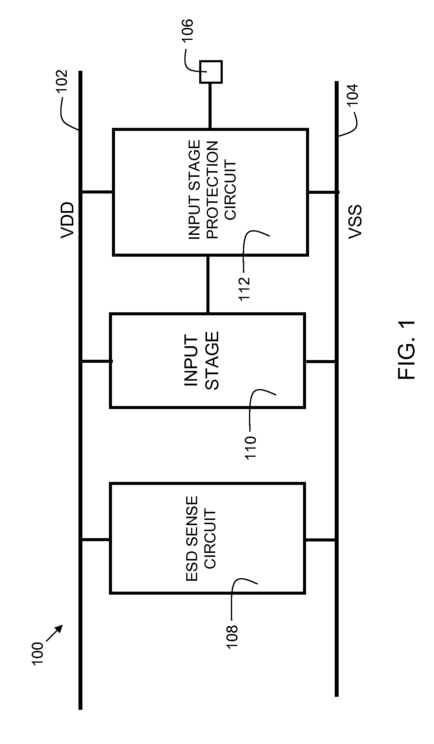
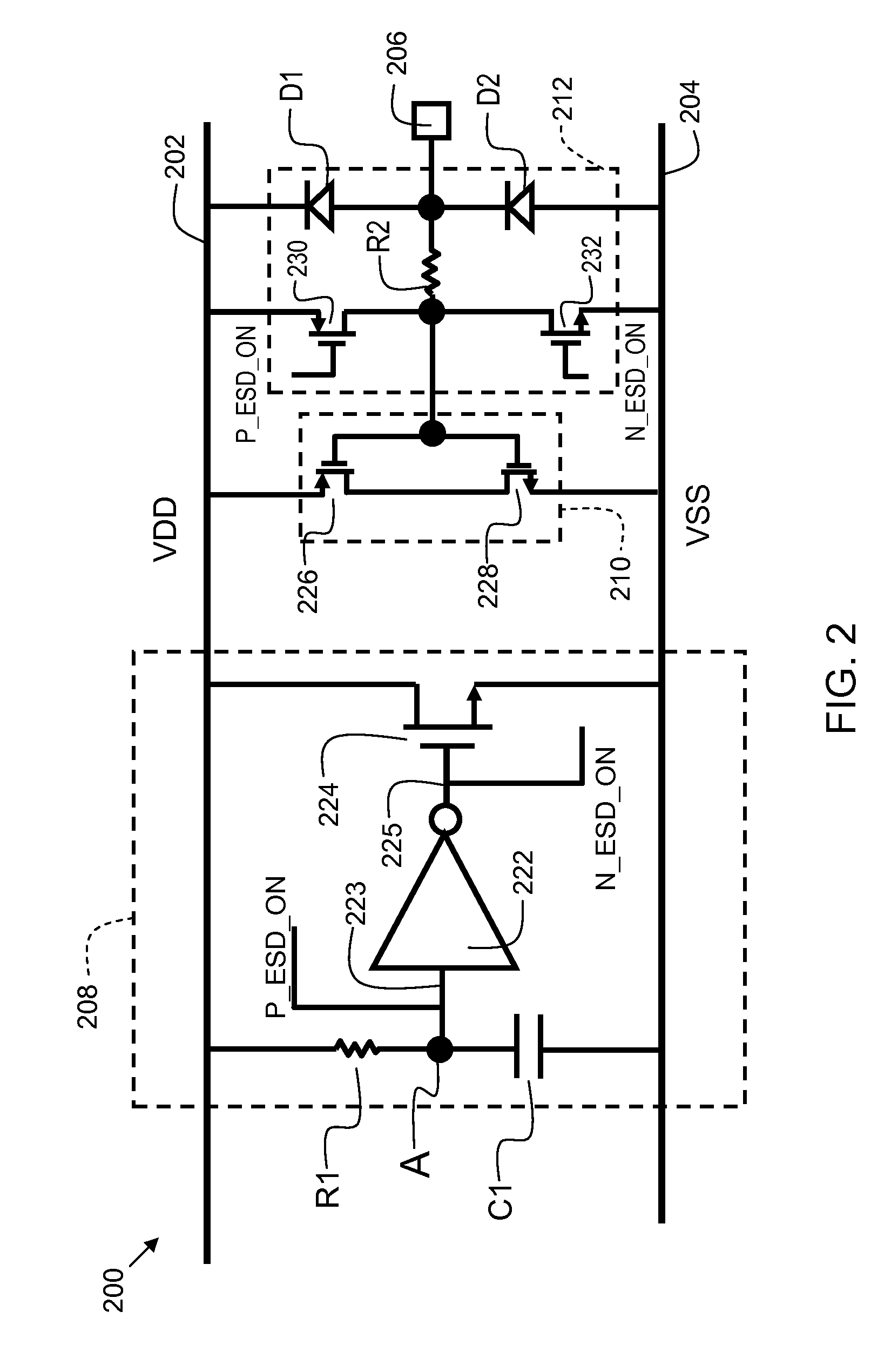
[0018]Exemplary embodiments will now be described more fully herein with reference to the accompanying drawings, in which exemplary embodiments are shown. Embodiments of the present invention provide a circuit for ESD protection. The circuit includes multiple transistors that are selectively turned on during an ESD event. An ESD sense circuit detects an ESD event and asserts signals to activate an ESD protection circuit which closes multiple protection transistors to dissipate current during the ESD event. During normal operation of the circuit, the signals are de-asserted, disabling the ESD protection circuit.

[0019]It will be appreciated that this disclosure may be embodied in many different forms and should not be construed as limited to the exemplary embodiments set forth herein. Rather, these exemplary embodiments are provided so that this disclosure will be thorough and complete and will fully convey the scope of this disclosure to those skilled in the art. The terminology used...


PUM


Abstract

A circuit for electrostatic discharge (ESD) protection is disclosed. The circuit includes multiple transistors that are selectively turned on during an ESD event. An ESD sense circuit detects an ESD event and asserts signals to activate an ESD protection circuit which closes multiple protection transistors to dissipate current during the ESD event. During normal operation of the circuit, the signals are de-asserted, disabling the ESD protection circuit.

Description

FIELD OF THE INVENTION[0001]The present invention relates generally to semiconductors and, more particularly, to a circuit for electrostatic discharge protection in semiconductors.BACKGROUND[0002]ESD (Electrostatic Discharge) protection design is a major factor in the reliability of deep-submicron CMOS Integrated Circuits (ICs). Since CMOS development technology is aggressive in the deep-submicron category, the device size and the thickness of the gate oxide are being continually reduced to improve the operating speed of the CMOS devices and integration density of the ICs. These highly scaled-down devices, however, have been found to be increasingly vulnerable to ESD. Therefore, ESD protection circuits have been added into the CMOS IC's to protect the IC's against ESD damage.[0003]As a result of detailed investigations of ESD events on IC products, it is known that there are three main types of ESD events: Human-Body Model (HBM), Machine Model (MM), and Charge Device Model (CDM). Th...

Claims


Application Information

Patent Timeline
Patent Type & Authority Patents(United States)
IPC IPC(8): H02H9/00H02H3/22H02H9/06H02H1/04H02H9/04
CPCH02H9/046
Inventor PRABHU, MANJUNATHA GOVINDANATARAJAN, MAHADEVA IYER
Owner GLOBALFOUNDRIES INC
Why Eureka
Try Eureka