Differential silicon oxide etch

a technology of silicon oxide and etching layer, applied in the direction of electrical discharge tubes, decorative arts, electrical apparatus, etc., can solve the problems of deformation of remaining materials, local plasma damage to substrates, wet processes cannot penetrate some constrained trenches, etc., and achieve the effect of less high density silicon and low density

Active Publication Date: 2015-05-19
APPLIED MATERIALS INC
View PDF713 Cites 174 Cited by
  • Summary
  • Abstract
  • Description
  • Claims
  • Application Information

AI Technical Summary

Problems solved by technology

However, wet processes are unable to penetrate some constrained trenches and sometimes deform the remaining material.
However, local plasmas can damage the substrate through the production of electric arcs as they discharge.
The Siconi™ etch is largely conformal and selective towards silicon oxide layers but does not readily etch silicon regardless of whether the silicon is amorphous, crystalline or polycrystalline.

Method used


Image

  • Differential silicon oxide etch
  • Differential silicon oxide etch
  • Differential silicon oxide etch

Examples


Embodiment Construction

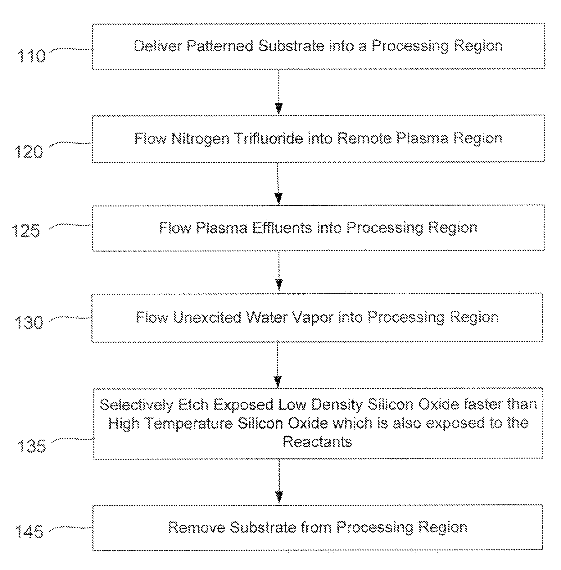
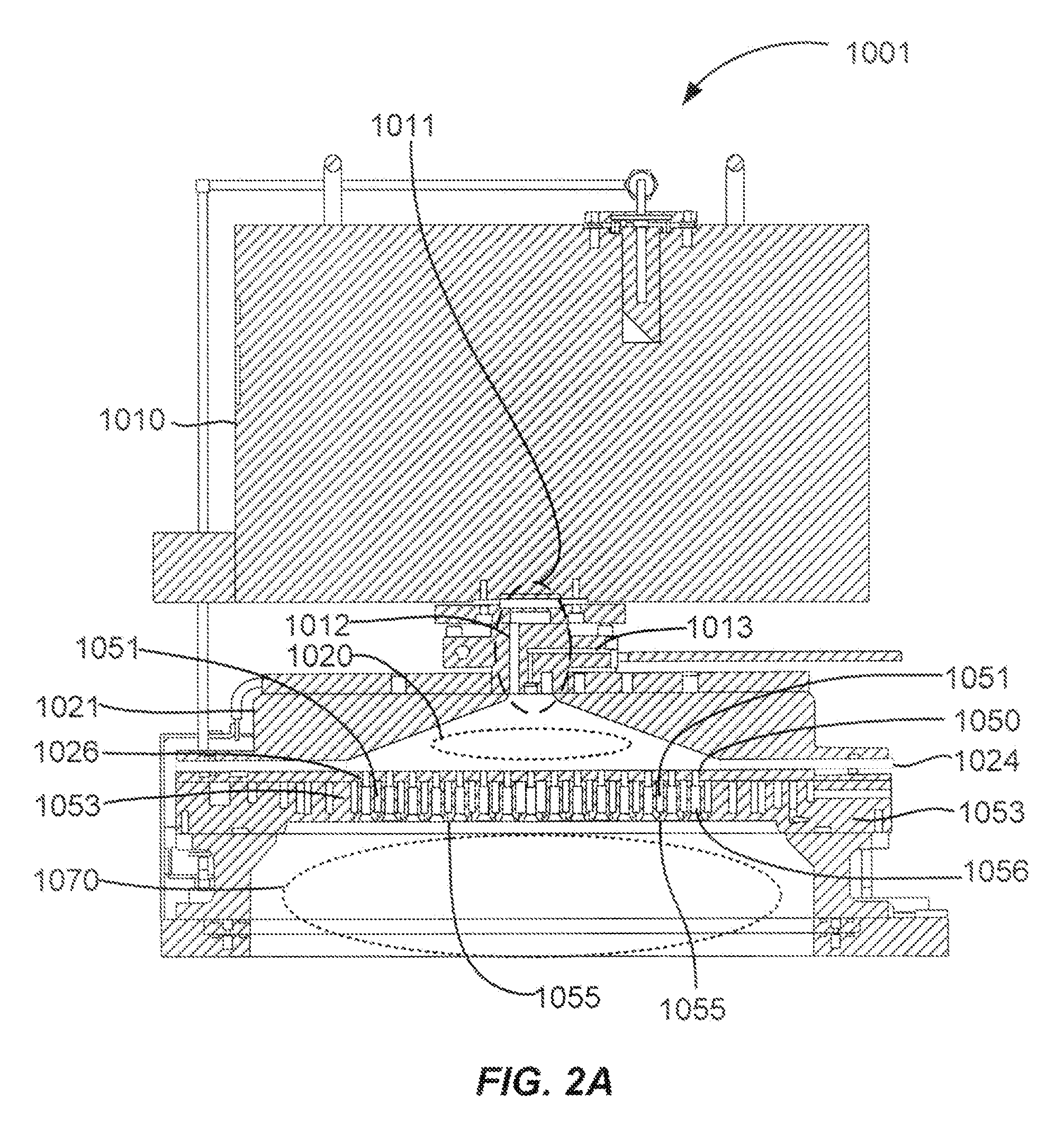
[0015]A method of etching exposed silicon oxide on patterned heterogeneous structures is described and includes a gas phase etch created from a remote plasma etch. The remote plasma excites a fluorine-containing precursor. Plasma effluents from the remote plasma are flowed into a substrate processing region where the plasma effluents combine with water vapor. Reactants thereby produced etch the patterned heterogeneous structures to remove two separate regions of differing silicon oxide at different etch rates. The methods may be used to remove low density silicon oxide while removing less high density silicon oxide.

[0016]Selective remote gas phase etch processes have used a hydrogen source of ammonia (NH3) and a fluorine source of nitrogen trifluoride (NF3) which together flow through a remote plasma system (RPS) and into a reaction region. The flow rates of ammonia and nitrogen trifluoride are typically chosen such that the atomic flow rate of hydrogen is roughly twice that of fluo...


PUM

PropertyMeasurementUnit
temperatureaaaaaaaaaa

Abstract

A method of etching exposed silicon oxide on patterned heterogeneous structures is described and includes a gas phase etch created from a remote plasma etch. The remote plasma excites a fluorine-containing precursor. Plasma effluents from the remote plasma are flowed into a substrate processing region where the plasma effluents combine with water vapor. Reactants thereby produced etch the patterned heterogeneous structures to remove two separate regions of differing silicon oxide at different etch rates. The methods may be used to remove low density silicon oxide while removing less high density silicon oxide.

Description

CROSS-REFERENCES TO RELATED APPLICATIONS[0001]This application claims the benefit of U.S. Prov. Pat. App. No. 61 / 701,964 filed Sep. 17, 2012, and titled “DIFFERENTIAL SILICON OXIDE ETCH,” which is hereby incorporated herein in its entirety by reference for all purposes.BACKGROUND OF THE INVENTION[0002]Integrated circuits are made possible by processes which produce intricately patterned material layers on substrate surfaces. Producing patterned material on a substrate requires controlled methods for removal of exposed material. Chemical etching is used for a variety of purposes including transferring a pattern in photoresist into underlying layers, thinning layers or thinning lateral dimensions of features already present on the surface. Often it is desirable to have an etch process which etches one material faster than another helping e.g. a pattern transfer process proceed. Such an etch process is said to be selective to the first material. As a result of the diversity of material...

Claims


Application Information

Patent Timeline
Patent Type & Authority Patents(United States)
IPC IPC(8): H01L21/302H01L21/461H01J37/32H01L21/3065H01L21/311
CPCH01L21/3065H01J37/32357H01L21/31116H01J37/32091H01J37/3244
Inventor PARK, SEUNG H.WANG, YUNYUZHANG, JINGCHUNWANG, ANCHUANINGLE, NITIN K.
Owner APPLIED MATERIALS INC
Why Eureka
Try Eureka