Semiconductor light emitting element

a technology of light-emitting elements and semiconductors, which is applied in the direction of basic electric elements, semiconductor devices, electrical equipment, etc., can solve problems such as discontinuity of wiring layers, and achieve the effect of high emission strength and high quality

Active Publication Date: 2015-05-26
NICHIA CORP
View PDF40 Cites 4 Cited by
  • Summary
  • Abstract
  • Description
  • Claims
  • Application Information

AI Technical Summary

Benefits of technology

[0010]As a result, the inventors perfected a semiconductor light emitting element that gives uniformly high emission strength and with which high quality, no discontinuity of the wiring layer, etc. is ensured, even when there is a wiring layer that conforms to bumps in the bottom face of the grooves, by keeping the width of the grooves that expose the convex portions of the substrate surface used for separation to a minimum.
[0013]According to the present invention, a semiconductor light emitting element that gives uniformly high emission strength and with which high quality, no discontinuity of the wiring layer, etc. is ensured can be realized.

Problems solved by technology

The inventors conducted diligent research into the above problem, and discovered that thinning of the wiring layer is apt to occur at the plurality of convex portions on the substrate surface, and particularly at places corresponding to the sides of the convex portions, and that this can lead to discontinuity of the wiring layer.

Method used


Image

  • Semiconductor light emitting element
  • Semiconductor light emitting element
  • Semiconductor light emitting element

Examples


embodiment 1

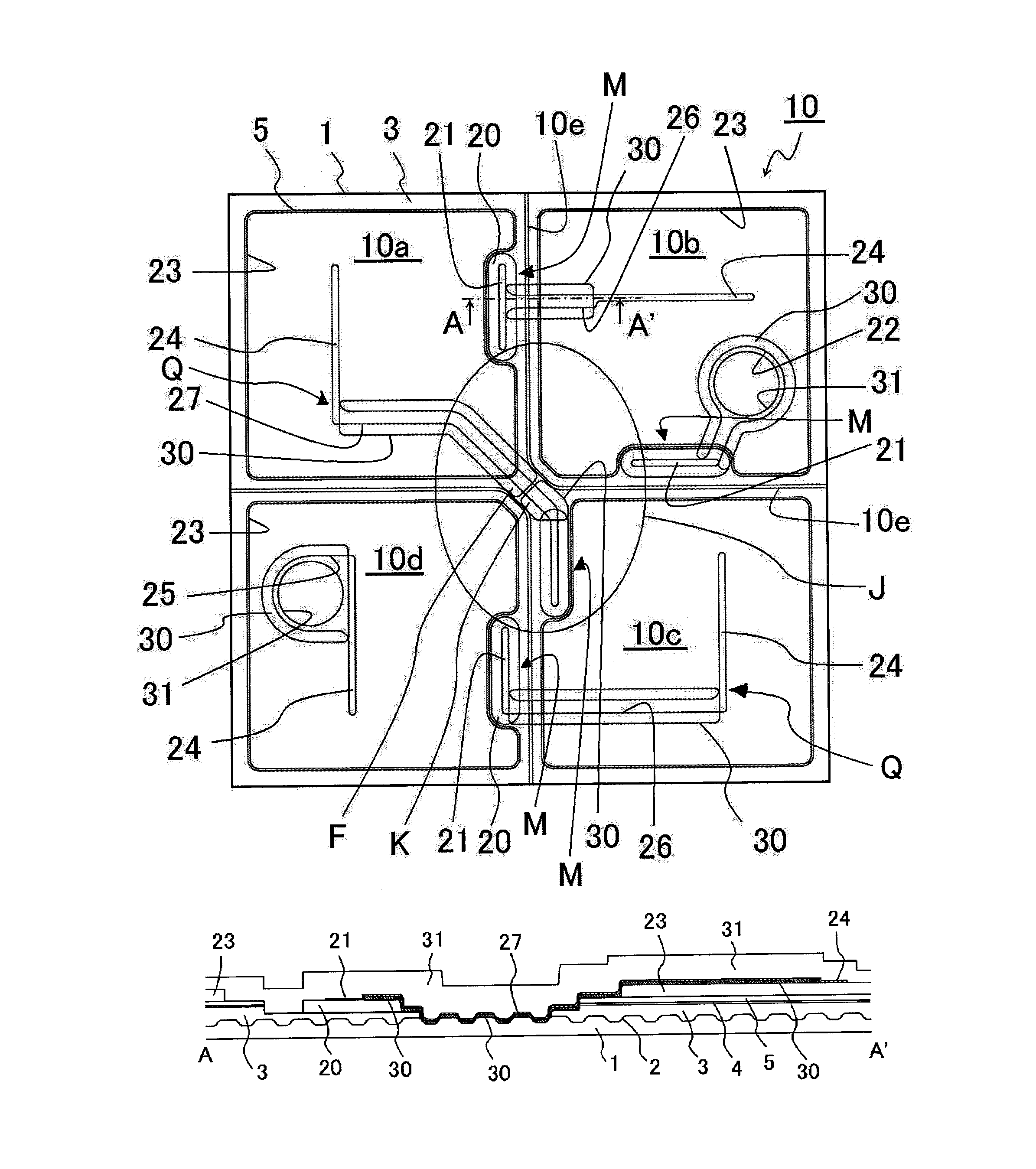
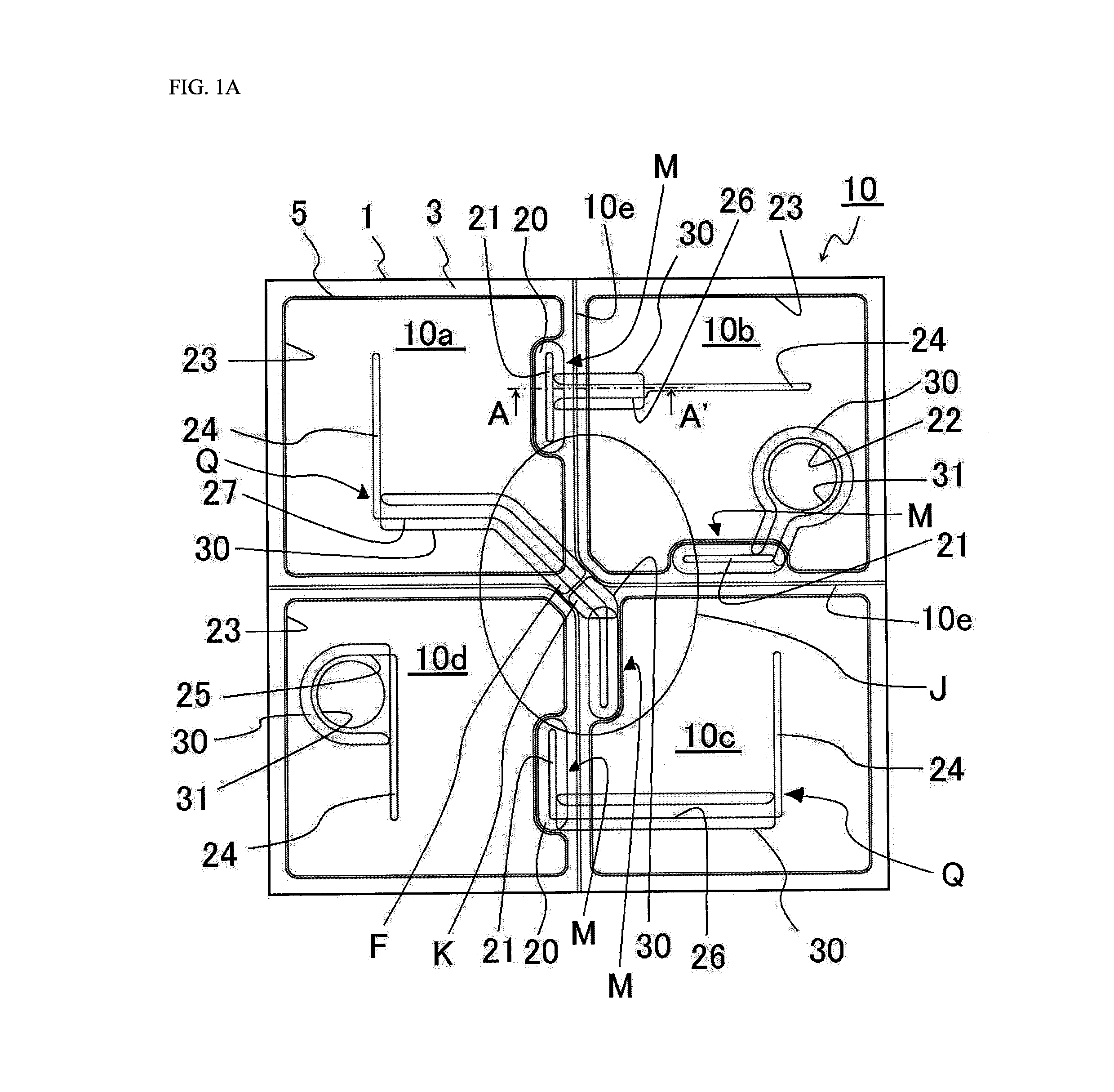
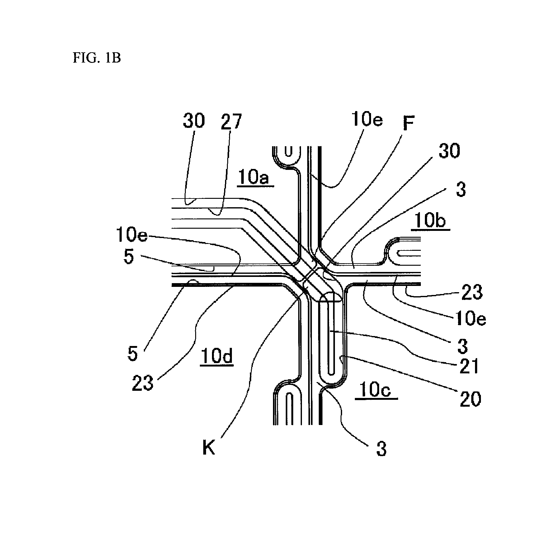
[0125]The semiconductor light emitting element of Embodiment 1 is shown in FIGS. 1A to 1E. In FIGS. 1A to 1E, however, for the sake of the description, the convex portions on the substrate surface discussed below are omitted in FIGS. 1A to 1C and 1F, and shown only in FIGS. 1D and 1E, and are exaggerated in FIG. 1D. FIG. 1G is a cross section along the B-B′ line in FIG. 1F, which is a plan view just as is FIG. 1A, in order to clarify the cut location in the plan view of the semiconductor light emitting element shown in FIG. 1A.

[0126]This semiconductor light emitting element 10 has four light emitting element components 10a to 10d, which are substantially square in shape, on a sapphire substrate 1.

[0127]As shown in FIGS. 1D and 1E in particular, the sapphire substrate 1 has a plurality of convex portions 2 on its surface. The convex portions 2 here are such that the basic shape of their bottom face is that of a regular triangle, the sides of which are rounded to form an outward bulge...

embodiment 2

[0158]The semiconductor light emitting element in Embodiment 2 is shown in FIG. 2A.

[0159]The semiconductor light emitting element 10A in this embodiment is configured the same as the semiconductor light emitting element 10 in Embodiment 1, except that the width of the grooves varies with their location.

[0160]With this semiconductor light emitting element 10A, grooves 11 having a relatively narrow width N are disposed between the light emitting element component 10a and the light emitting element component 10d, and between the light emitting element component 10b and the light emitting element component 10c. Grooves 12 having a relatively wide width M are disposed between the light emitting element component 10a and the light emitting element component 10b, and between the light emitting element component 10d and the light emitting element component 10c. Also, a groove having a linear shape and extending diagonally from the light emitting element component 10d to the light emitting e...

embodiment 3

[0164]The semiconductor light emitting element in Embodiment 3 is shown in FIG. 2B.

[0165]The semiconductor light emitting element 10B in this embodiment is configured the same as the semiconductor light emitting element 10 in Embodiment 1, except that the width of the grooves varies with their location.

[0166]With the semiconductor light emitting element 10B in this embodiment, grooves 11 having a relatively narrow width N are disposed between the light emitting element component 10a and the light emitting element component 10d, and between the light emitting element component 10b and the light emitting element component 10c.

[0167]Grooves 14, which have a relatively wide width W at the places where the second connector 26 is disposed extending in the column direction, and elsewhere has a relatively narrow width R, are disposed between the light emitting element component 10a and the light emitting element component 10b, and between the light emitting element component 10d and the li...


PUM


Abstract

A semiconductor light emitting element includes: an insulating substrate having a plurality of convex portions on a surface thereof; a plurality of light emitting element components having semiconductor laminated bodies that are laminated on the insulating substrate and are separated from one another by a groove that exposes the convex portions; and a connector connecting between the light emitting element components. The light emitting element components include a first light emitting element component and a second light emitting element component. The first light emitting element component is separated from the second light emitting element component with the groove in between, and has a first protrusion that protrudes toward the second light emitting element component. The connector includes a first connector having a shape that straddles the groove and that follows the convex portions, and has a straight section.

Description

CROSS-REFERENCE TO RELATED APPLICATIONS[0001]This application claims priority to Japanese Patent Applications No. 2013-14932, No. 2013-91224 and No. 2013-203610 filed on Jan. 30, 2013, Apr. 24, 2013 and Sep. 30, 2013, respectively. The entire disclosure of Japanese Patent Applications No. 2013-14932, No. 2013-91224 and No. 2013-203610 are hereby incorporated herein by reference.BACKGROUND OF THE INVENTION[0002]1. Background Information[0003]The present invention relates to a semiconductor light emitting element.[0004]2. Background Art[0005]A structure for a light emitting element that gives uniform light emission has been proposed in the past in which a semiconductor laminated body including an active layer laminated on a substrate having a surface with concavities and convexities is divided into a plurality of small regions, which are electrically connected and arranged longitudinally and / or laterally (e.g., JP2011-171739A).[0006]With this light emitting element structure, grooves ...

Claims


Application Information

Patent Timeline
Patent Type & Authority Patents(United States)
IPC IPC(8): H01L27/15H01L33/08H01L33/20H01L33/38H01L33/62
CPCH01L33/62H01L27/15H01L27/156H01L33/08H01L33/20H01L33/38H01L2933/0016H01L2924/0002H01L2924/00
Inventor EMURA, KEIJIMIYAGI, AKIHIROKITAHAMA, SHUN
Owner NICHIA CORP
Why Eureka
Try Eureka