Method for writing in and reading data from a semiconductor storage device and semiconductor storage device

a technology of semiconductor storage devices and data, applied in the direction of static storage, digital storage, instruments, etc., can solve the problems of improper determination and improper determination, and achieve the effect of preventing improper determination and reducing the variation of readout curren

Active Publication Date: 2015-05-26
LAPIS SEMICON CO LTD
View PDF12 Cites 0 Cited by
  • Summary
  • Abstract
  • Description
  • Claims
  • Application Information

AI Technical Summary

Benefits of technology

[0012]The present invention has been developed in view of such problems. It is therefore an object of the invention to provide a method for writing data in a semiconductor storage device and a semiconductor storage device which can reduce a variation in the readout current from a sub storage region serving as a reference cell of memory cells of the semiconductor storage device, thereby preventing an improper determination from being made about the readout current from a memory cell.
[0015]According to the method for writing data in the semiconductor storage device of the present invention, data is written into a memory cell in the two data write steps in which the magnitudes of the voltages applied to the first impurity region and the second impurity region of a memory cell are different from each other. Thus, the semiconductor storage device and the method for writing data in the semiconductor storage device are provided which allow charge to be accumulated in the first charge accumulation portion and the second charge accumulation portion to reduce variations in readout current from the memory cells of the semiconductor storage device, thereby preventing an improper determination from being made when determining the readout current from the memory cells.

Problems solved by technology

As such, a variation in the amount of charge accumulated in the nitride film of the reference cell causes the readout current from the reference cell to be initially reduced, resulting in an improper determination being made when the readout currents are compared between the memory cell being read and the reference cell.
Such an improper determination may also be made even in the case of the memory cell disclosed in Document 1 cited above.

Method used


Image

  • Method for writing in and reading data from a semiconductor storage device and semiconductor storage device
  • Method for writing in and reading data from a semiconductor storage device and semiconductor storage device
  • Method for writing in and reading data from a semiconductor storage device and semiconductor storage device

Examples


embodiments

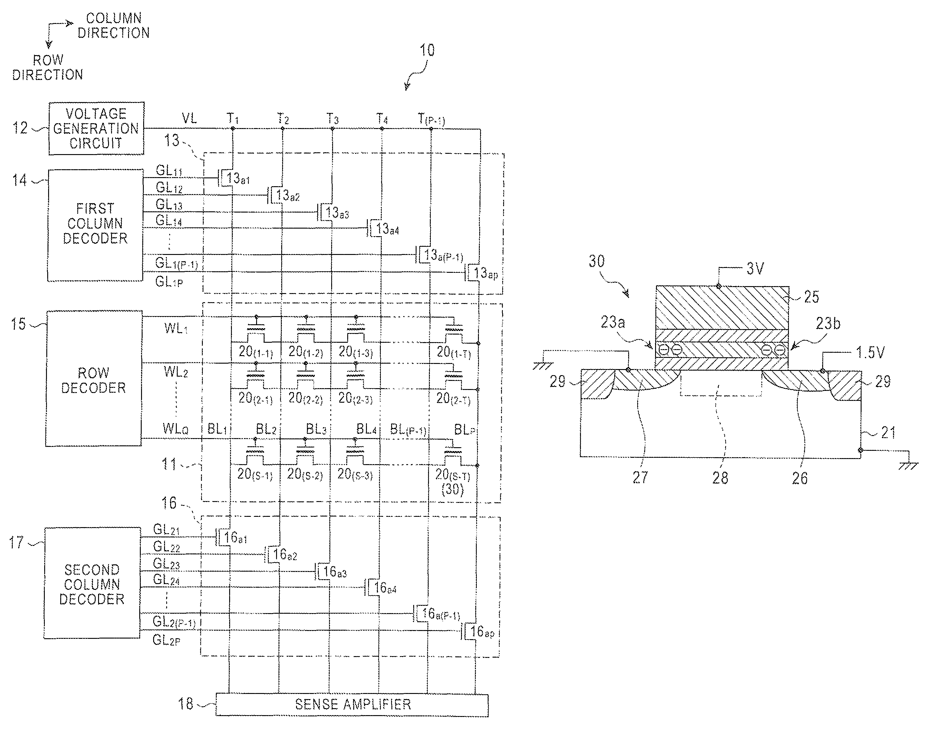
[0024]First, referring to FIG. 1, a description will be made to a semiconductor storage device according to an embodiment. FIG. 1 is a view illustrating the general configuration of a semiconductor storage device according to the present embodiment.

[0025]As shown in FIG. 1, a semiconductor storage device 10 includes a memory array 11 made up of a plurality of memory cells; a voltage generation circuit 12 for generating a voltage to be supplied to the memory array 11; a first group of switching elements 13 provided between the memory array 11 and the voltage generation circuit 12; a first column decoder 14 for supplying a driving signal to the first group of switching elements 13; a row decoder 15 for supplying a driving signal to the memory array 11; a second group of switching elements 16 connected to the memory array 11; a second column decoder 17 for supplying a driving signal to the second group of switching elements 16; and a sense amplifier 18 connected to the second group of ...


PUM


Abstract

A method for writing data in a semiconductor storage device and a semiconductor storage device are provided, that can reduce variations in readout current from a sub storage region which serves as a reference cell for the memory cells of the semiconductor storage device, thereby preventing an improper determination from being made when determining the readout current from a memory cell. In the method, data is written on a memory cell in two data write steps by applying voltages to the first and second impurity regions of the memory cell, the voltages being different in magnitude from each other.

Description

BACKGROUND OF THE INVENTION[0001]1. Field of the Invention[0002]The present invention relates to a method for writing reference data in a sub storage region of a semiconductor storage device and to a semiconductor storage device which has the reference data written therein.[0003]2. Description of the Related Art[0004]Memory devices used for various types of electronic devices for handling digital information can be largely classified into a group of storage devices such as hard disk drives, DVDs, and CDs, which require physical operations; and another group of storage devices equipped with a semiconductor memory device which requires no physical operations. The semiconductor memory device can be further classified into two types according to the method of sustaining stored data. More specifically, the semiconductor memory device can be classified into a volatile semiconductor memory device in which stored information will vanish when the power supply is turned off and a nonvolatile ...

Claims


Application Information

Patent Timeline
Patent Type & Authority Patents(United States)
IPC IPC(8): G11C16/04G11C7/06G11C16/14G11C16/34
CPCG11C16/0466G11C16/34G11C16/0483G11C16/14G11C16/04G11C7/062
Inventor SAEKI, KATSUTOSHI
Owner LAPIS SEMICON CO LTD
Why Eureka
Try Eureka