Semiconductor memory device and operation method thereof

a technology of semiconductor memory and operation method, which is applied in the direction of digital storage, data conversion, instruments, etc., can solve the problems of data storage completion time and hinder the obtaining and achieve the effect of high speed operation of semiconductor memory device and short storage completion tim

Inactive Publication Date: 2015-05-26
SK HYNIX INC
View PDF8 Cites 0 Cited by
  • Summary
  • Abstract
  • Description
  • Claims
  • Application Information

AI Technical Summary

Benefits of technology

[0019]The semiconductor memory device in accordance with the embodiment of the present invention includes storage units having a short storage completion time. The embodiment of the present invention stores sequentially input information data in a corresponding storage unit based on selection signals that are sequentially activated, thereby enabling a data storage operation of mode register units regardless of the data storage completion time of the mode register units.
[0020]According to the embodiment of the present invention, it is possible to sequentially store input data regardless of the data storage completion time of the mode registers. Therefore, a high speed operation of the semiconductor memory device may be obtained.

Problems solved by technology

However, obtaining a high speed operation of the semiconductor memory device may be hindered by data storage completion times of mode registers.

Method used


Image

  • Semiconductor memory device and operation method thereof
  • Semiconductor memory device and operation method thereof
  • Semiconductor memory device and operation method thereof

Examples


Embodiment Construction

[0027]Exemplary embodiments of the present invention will be described below in more detail with reference to the accompanying drawings. The present invention may, however, be embodied in different forms and should not be construed as limited to the embodiments set forth herein. Rather, these embodiments are provided so that this disclosure will be thorough and complete, and will fully convey the scope of the present invention to those skilled in the art. Throughout the disclosure, like reference numerals refer to like parts throughout the various figures and embodiments of the present invention.

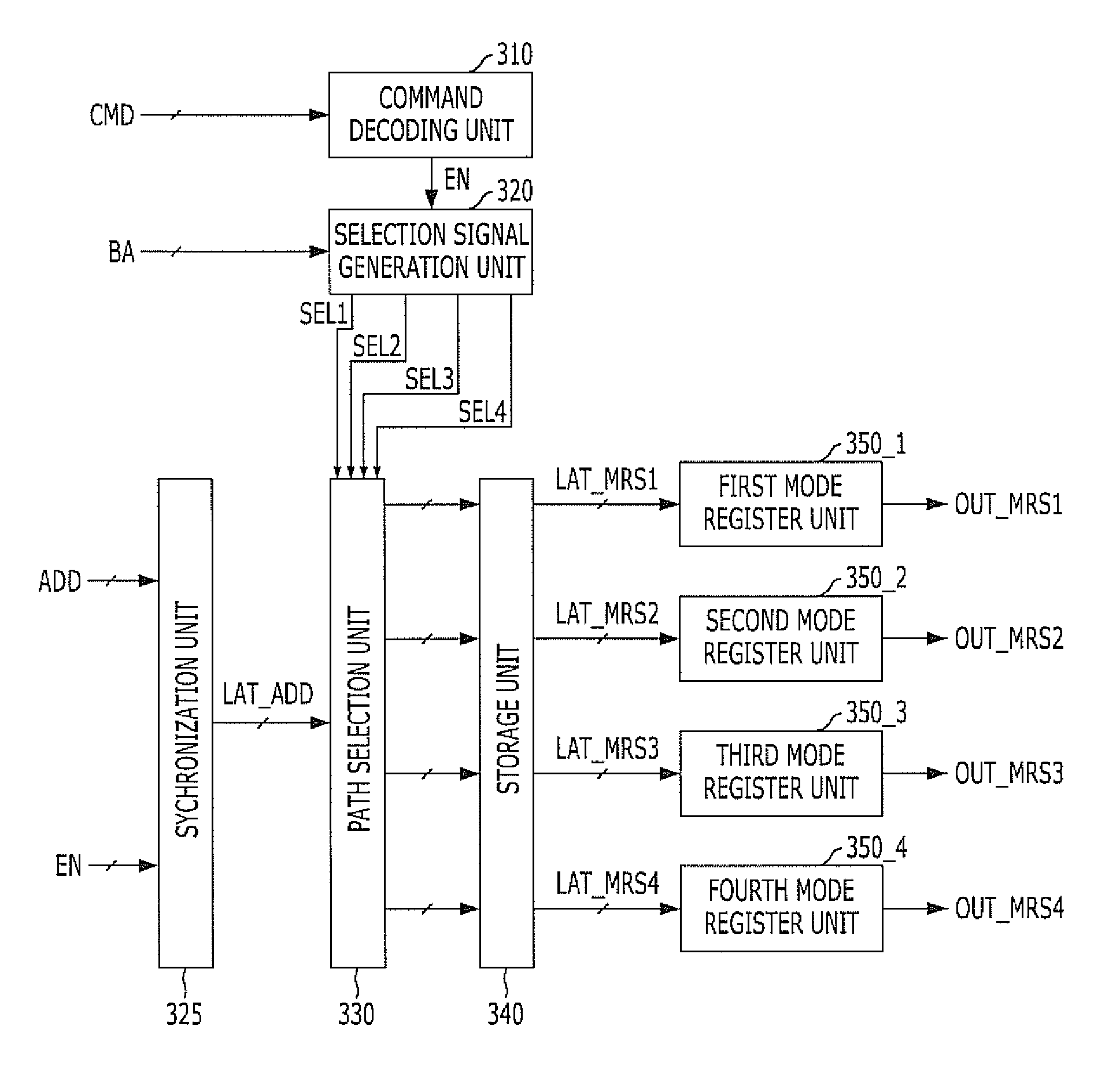
[0028]FIG. 3 is a block diagram for illustrating a partial configuration of a semiconductor memory device in accordance with an embodiment of the present invention.

[0029]Referring to FIG. 3, the semiconductor memory device includes a command decoding unit 310, a selection signal generation unit 320, a synchronization unit 325, a path selection unit 330, a storage unit 340, and first to fourt...


PUM


Abstract

A semiconductor memory device includes a selection signal generation unit configured to generate a plurality of selection signals that are sequentially activated, a path selection unit configured to select a transmission path of sequentially input information data in response to the plurality of selection signals, a plurality of first storage units, each configured to have a first storage completion time and store an output signal of the path selection unit, and a plurality of second storage units, each configured to have a second storage completion time, which is longer than the first storage completion time, and store a respective output signal of the plurality of first storage units.

Description

CROSS-REFERENCE TO RELATED APPLICATIONS[0001]The present application claims priority of Korean Patent Application No. 10-2011-0110498, filed on Oct. 27, 2011, which is incorporated herein by reference in its entirety.BACKGROUND[0002]1. Field[0003]Exemplary embodiments of the present invention relate to a semiconductor design technology, and more particularly, to a semiconductor memory device provided with mode register units.[0004]2. Description of the Related Art[0005]In general, a semiconductor memory device such as a double data rate synchronous DRAM (DDR SDRAM) is provided with mode register units, wherein the mode register units store information of device operation, such as CAS latency, column address strobe latency, a bust type, a burst length, a bank grouping mode, and DLL on / off. The mode register units store corresponding information before the semiconductor memory device operates, and the semiconductor memory device is set with the stored information. The information data...

Claims


Application Information

Patent Timeline
Patent Type & Authority Patents(United States)
IPC IPC(8): G06F3/00G06F5/00G11C7/10G11C11/4072
CPCG11C11/4072G11C7/1045G11C8/04G11C8/10
Inventor KIM, TAE-KYUN
Owner SK HYNIX INC
Why Eureka
Try Eureka