Method of detecting transistors mismatch in a SRAM cell

a technology of sram cell and transistor, which is applied in the field of semiconductor fabrication technology, can solve the problems of reducing product yield, inconvenient mass data collection, and time-consuming methods, and achieves the effect of reducing the cost of mass statistical analysis by the conventional positioning and measuring device, and achieving quick and convenient determination

Active Publication Date: 2015-06-16
SHANGHAI HUALI MICROELECTRONICS CORP
View PDF6 Cites 0 Cited by
  • Summary
  • Abstract
  • Description
  • Claims
  • Application Information

AI Technical Summary

Benefits of technology

[0015]In the present invention, the mismatched transistors in the SRAM cell can be determined quickly and conveniently, the cost of the mass statistical analysis by the conventional positioning and measuring devices can also be reduced.

Problems solved by technology

According to the SRAM cell manufacturing process currently, with the decrease of the minimum supply voltage (Vmin), the mismatch between the transistors in the SRAM cell occurs more frequently, and thus decrease the product yield.
However, such method is time-consuming, costly, and inconvenient for mass data collection.

Method used


Image

  • Method of detecting transistors mismatch in a SRAM cell
  • Method of detecting transistors mismatch in a SRAM cell
  • Method of detecting transistors mismatch in a SRAM cell

Examples


Embodiment Construction

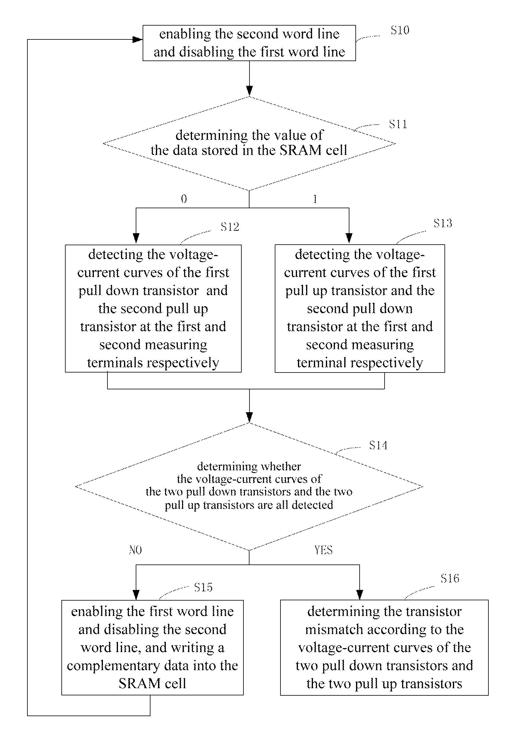
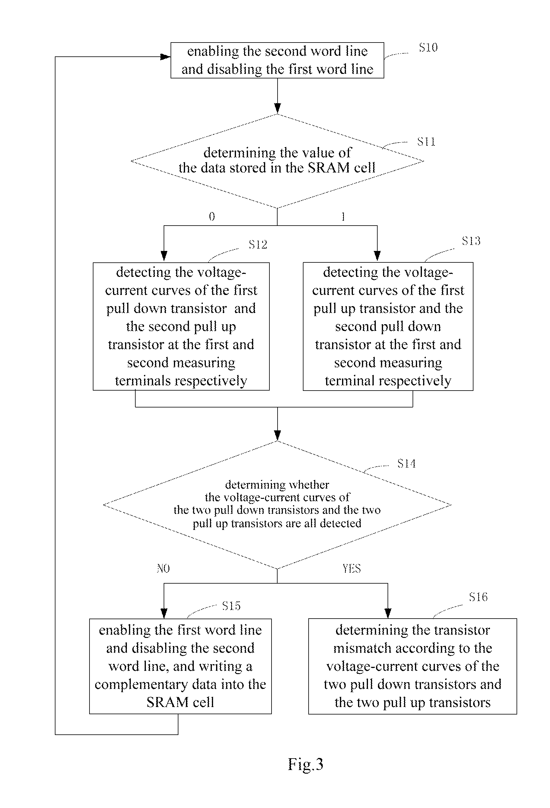
[0020]Reference will now be made in detail to the present preferred embodiments and the accompanying figures of the invention in order to provide a further understanding of the invention. The figures are not drawn to scale and they are provided merely to illustrate the invention instead of limiting the scope of the present invention, like reference numerals are used throughout the figures to designate similar or equivalent element.

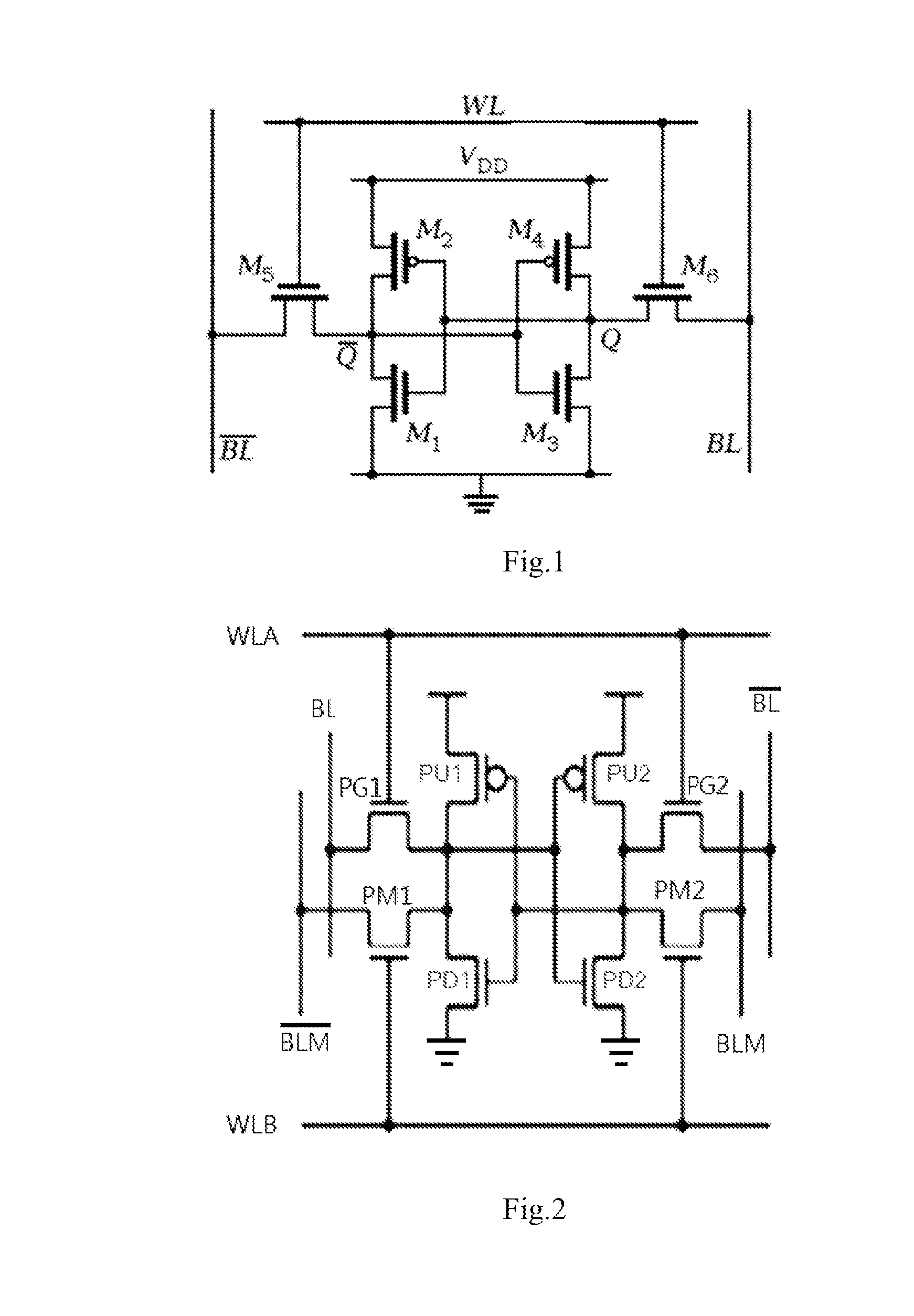
[0021]FIG. 2 is a schematic diagram of a SRAM cell to be detected in an embodiment of the present invention.

[0022]The SRAM cell comprises a first and a second pull up transistors (PU1, PU2), a first and a second pull down transistors (PD1, PD2), a first and a second pass-gate transistors (PG1, PG2). The first and second pull up transistors (PU1, PU2), the first and the second pull down transistors (PD1, PD2) form a bi-stable circuit for data (“0” or “1”) latching. The gate electrodes of the first and second pass-gate transistors (PG1, PG2) are connected to...


PUM


Abstract

The present invention provides a method of detecting the transistor mismatch in a SRAM cell. The SRAM cell comprises two pass-gate transistors and a bi-stable circuit including two pull up transistors and two pull down transistors. The method comprises: providing two measuring transistors, whose gates are connected to a second word line, sources are connected to the outputs of the bi-stable circuit respectively and drains are connected to two measuring terminals respectively; turning on the measuring transistors and turning off the pass-gate transistors; detecting the voltage-current curve of the two pull down transistors and the two pull up transistors through the measuring transistors at the measuring terminals so as to detect the transistor mismatch in the SRAM cell.

Description

CROSS-REFERENCE TO RELATED APPLICATION[0001]This application claims the priority benefit of China application serial no. 201310317737.1, filed Jul. 25, 2013. All disclosure of the China application is incorporated herein by reference.FIELD OF THE INVENTION[0002]The present invention relates to the field of semiconductor fabrication technology and particularly to a method of detecting the transistors mismatch in a SRAM cell.BACKGROUND OF THE INVENTION[0003]The SRAM (static random access memory), which is a memory cell, is widely applied in the personal communications or consumer electronics with its characteristic of high speed and low power consumption.[0004]As shown in FIG. 1, a conventional 6T SRAM cell is structurally symmetrical, which is consist of six transistors M1, M2, M3, M4, M5 and M6. Wherein, the transistors M1, M2 M3 and M4 form a bi-stable circuit to latch a digital signal. The transistors M5 and M6 are Pass-Gate transistors to connect or disconnect the SRAM cell with ...

Claims


Application Information

Patent Timeline
Patent Type & Authority Patents(United States)
IPC IPC(8): G11C29/50G11C11/417G11C11/41
CPCG11C29/50008G11C11/417G11C2029/5004G11C2029/5006G11C11/41G11C2029/5002
Inventor CAI, ENJINGLI, QIANGWEI, WEN
Owner SHANGHAI HUALI MICROELECTRONICS CORP
Why Eureka
Try Eureka