Printed board arrangement

a printed circuit board and arrangement technology, applied in the field of electronic circuitry, can solve the problems of unsuitable printed circuit boards, tedious and susceptible to faults, and unsuitable connection techniques, and achieve the effect of simple and space-saving

Inactive Publication Date: 2015-06-16
HUBERSUHNER AG
View PDF20 Cites 0 Cited by
  • Summary
  • Abstract
  • Description
  • Claims
  • Application Information

AI Technical Summary

Benefits of technology

[0012]The object of the invention is therefore to provide a printed circuit board arrangement of the type mentioned initially, in which RF-compatible electrical connections are made between the printed circuit boards in a simple and space-saving manner when the printed circuit boards are fitted on the base plate, and without any need for further additional tasks or reworking, and which electrical connections are suitable for use as signal lines up to the extremely high frequency range of several GHz.

Problems solved by technology

Connection apparatuses which operate by means of pressure have already been proposed for the electrical connection of printed circuit boards arranged alongside one another, in U.S. Pat. No. 6,612,851, but these act on the upper face and lower face of the printed circuit boards and are therefore not suitable for printed circuit boards arranged on a base plate.
However, the connectors must be installed retrospectively and must be screwed to one or both printed circuit boards, which is tedious and susceptible to faults.
This connection technique is also unsuitable for printed circuit boards which rest on a base plate.

Method used


Image

  • Printed board arrangement
  • Printed board arrangement
  • Printed board arrangement

Examples


Embodiment Construction

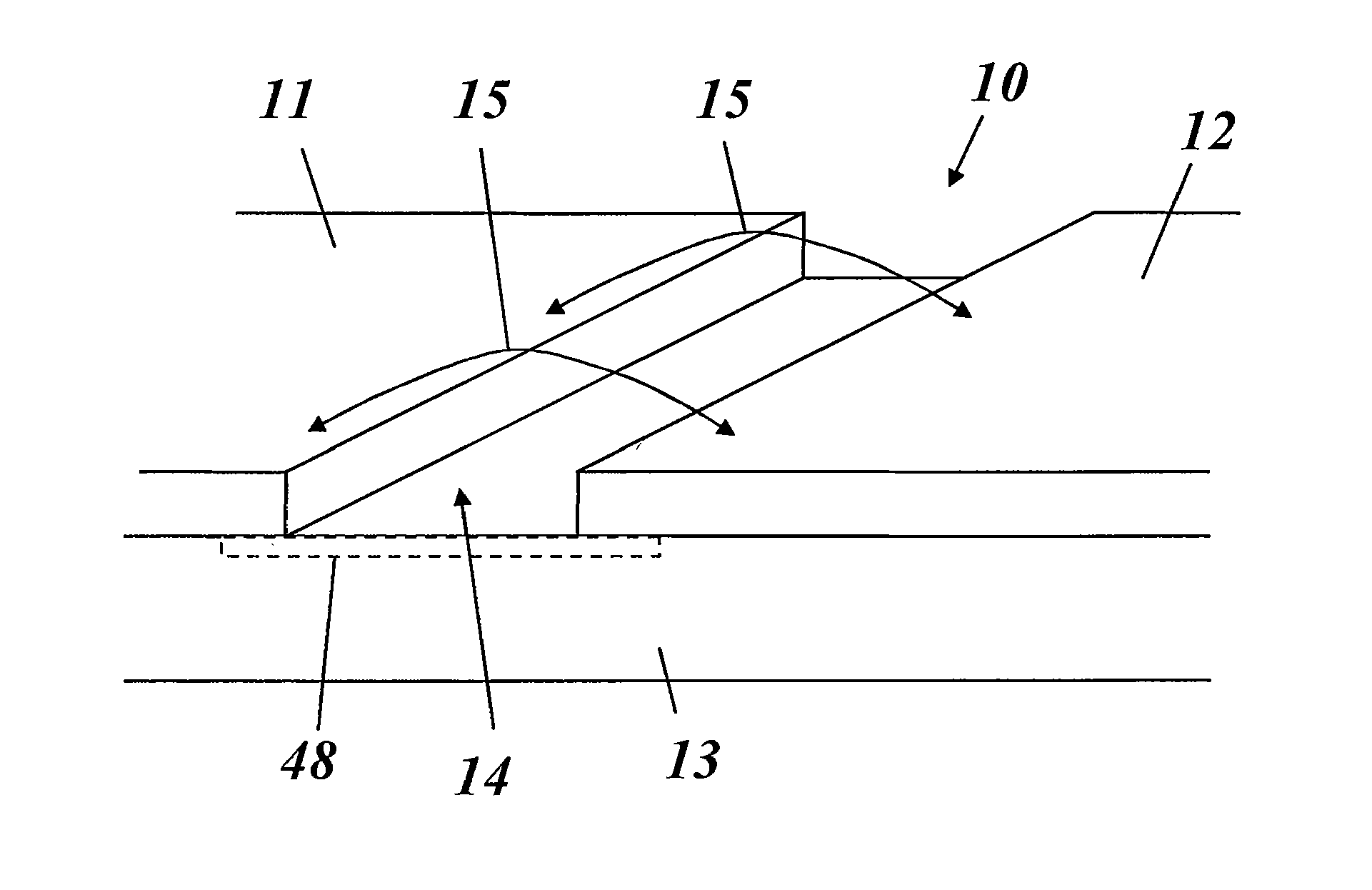
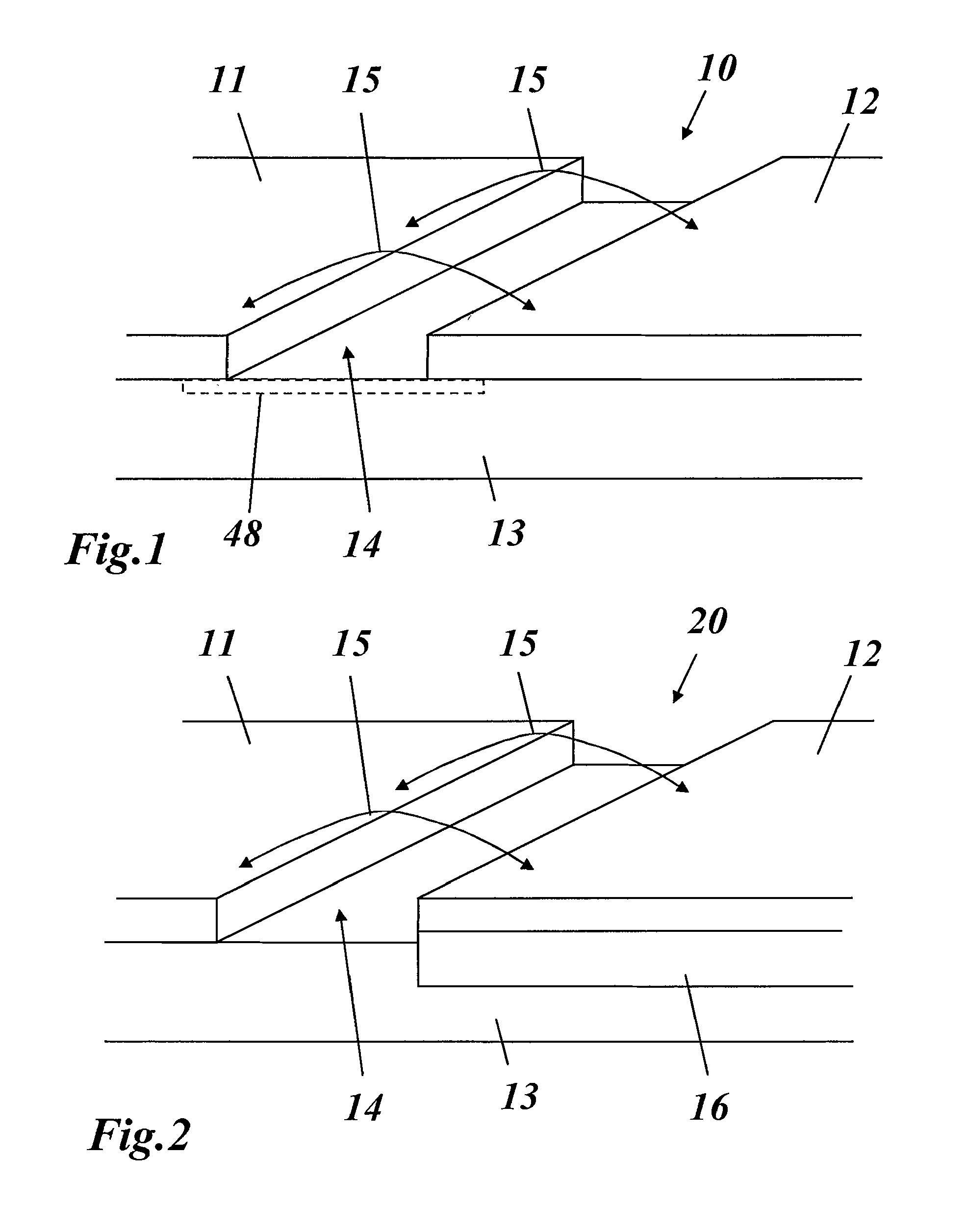
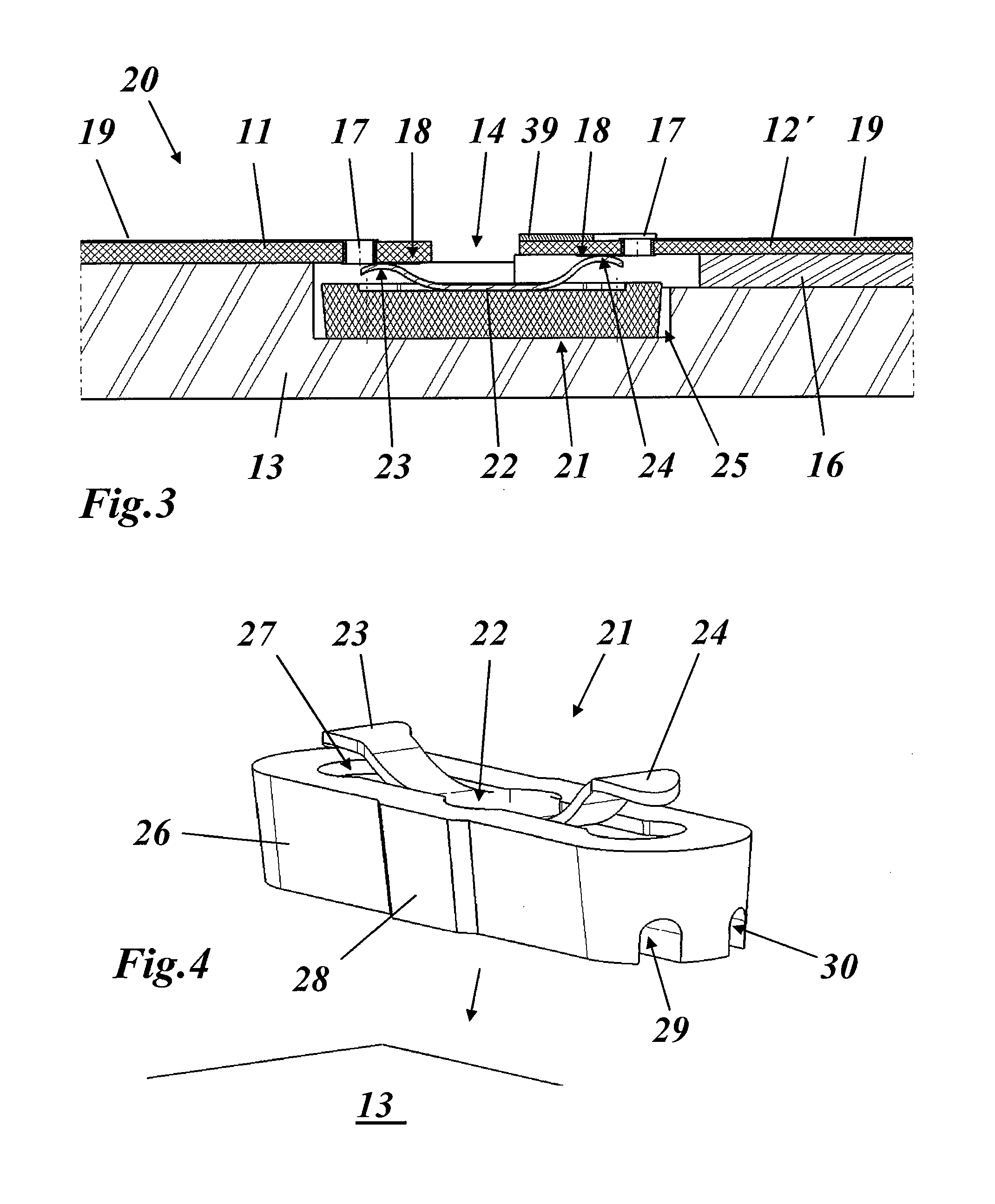
[0048]FIG. 3 shows a section illustration of a printed circuit board arrangement having two printed circuit boards, which are RF-connected via a contact-making element inserted into the base plate, according to a first exemplary embodiment of the invention. The printed circuit board arrangement 20, which has a base plate 13′ of stepped thickness based on the principle illustrated in FIG. 2, comprises two printed circuit boards 11 and 12′ of different thickness, with the thicker printed circuit board 12′ being designed for higher thermal loads by means of a thermal dissipation plate 16, as already mentioned initially, on the lower face. The two printed circuit boards 11 and 12′ rest, with a separation between them, on the base plate 13′ arranged underneath, such that an intermediate space 14 remains free, which is bridged by a contact-making element 21 for each signal line, for the electrical connection of the two printed circuit boards 11, 12′.

[0049]The contact-making element 21 in ...


PUM


Abstract

The invention relates to a printed circuit board arrangement (20) having at least two printed circuit boards (11; 12′), which are located alongside one another on a common, electrically conductive base plate (13′), have two mutually opposite edges, forming an intermediate space (14), and are connected to one another, bridging the intermediate space (14) by means of electrical connections (21), in order to transmit extremely high frequencies. In the case of a printed circuit board arrangement such as this, RF-compatible electrical connections are made between the printed circuit boards in a simple and space-saving manner when the printed circuit boards are fitted on the base plate and without any further necessary additional tasks or reworking, in that the electrical connections are each made via at least one contact-making element (21), via which the printed circuit boards make detachable electrical contact with one another when mounted on the base plate (13′).

Description

BACKGROUND OF THE INVENTION[0001]1. Field of the Invention[0002]The present invention relates to the field of electronic circuitry in the extremely high frequency region, in the range of operating frequencies up to several GHz. It relates in particular to a printed circuit board arrangement according to the precharacterizing clause of claim 1.[0003]In modern communications technology and in other fields which operate using extremely high frequency, electronic circuits are formed on printed circuit boards (PCBs) which have one or more conductor layers on an electrically insulating supporting board, which conductor layers are structured at least in places and form conductor tracks or surfaces which connect electronic components which are fitted and / or soldered to the supporting board to one another and / or to the outside world.[0004]In the case of relatively large appliance units such as base stations for mobile radio technology, a plurality of separate printed circuit boards are accom...

Claims


Application Information

Patent Timeline
Patent Type & Authority Patents(United States)
IPC IPC(8): H01R12/00H05K3/36H01R12/73H05K1/14
CPCH05K3/368H01R12/732H01R12/73H05K1/14H05K2201/10265
Inventor WAGNER, MARTINFUCHS, JOSEF
Owner HUBERSUHNER AG
Why Eureka
Try Eureka