TID hardened and single event transient single event latchup resistant MOS transistors and fabrication process

a technology of mos transistor and latchup resistance, which is applied in the field ofmos technology and radiation hardened mos transistor, can solve the problems of limited recovery from strike, and achieve the effects of less resistive, reduced impedance, and same junction breakdown performan

Active Publication Date: 2015-07-28
MICROSEMI SOC
View PDF19 Cites 2 Cited by
  • Summary
  • Abstract
  • Description
  • Claims
  • Application Information

AI Technical Summary

Benefits of technology

[0017]According to a first aspect of the present invention, a lateral n-p junction is created in the transistor to isolate the device channel from the sidewall of the STI isolation structure on both the source and drain regions of the transistor. Additional p-type implants may be added in this isolation ring to increase the parasitic Vt and improve TID immunity. The doping profile can be engineered so as not to degrade junction breakdown. In this embodiment of the present invention, the drain of the transistor is isolated from STI by a lateral junction.
[0019]According to another aspect of the present invention, additional p-type implants may be employed to increase TID immunity. The p-type implant may be separated from the edge of the n-type drain to preserve drain-body junction breakdown performance. The N+ source / drain implant is overlapped by a lighter n-type lightly-doped-drain (NLDD) implant, grading the n-type side of the junction. Similarly, the P+ body implant is overlapped by a lighter p-type lightly-doped-drain (PLDD) implant, grading the p-type side of the junction. In between is a region of very lightly-doped p-type high voltage p-well, further grading the p-type side of the diode. Finally, a higher energy p-type implant is added to provide improved conduction deeper near the N+ to high-voltage p-well junction.
[0021]According to another aspect of the present invention, the shallow-trench isolation between source / drain and body diffusions is replaced by an engineered junction. This butted junction greatly reduces the impedance from the source or drain to the body tap, while maintaining the same junction breakdown performance as the trench-isolated device. This scheme can be used to make the standard tap region or guard ring less resistive and more immune to set transient or latchup.
[0022]According to another aspect of the present invention, a salicided body (bulk) contact is located in a region of the engineered junction. This also reduces the impedance from the source or drain to the body tap, while maintaining the same junction breakdown performance as the trench-isolated device. This scheme can be used to make the standard tap region or guard ring less resistive and more immune to single event transient or single event latchup events.

Problems solved by technology

Recovery from the strike is limited by the impedance to the body tap.

Method used


Image

  • TID hardened and single event transient single event latchup resistant MOS transistors and fabrication process
  • TID hardened and single event transient single event latchup resistant MOS transistors and fabrication process
  • TID hardened and single event transient single event latchup resistant MOS transistors and fabrication process

Examples


Embodiment Construction

[0032]Persons of ordinary skill in the art will realize that the following description of the present invention is illustrative only and not in any way limiting. Other embodiments of the invention will readily suggest themselves to such skilled persons.

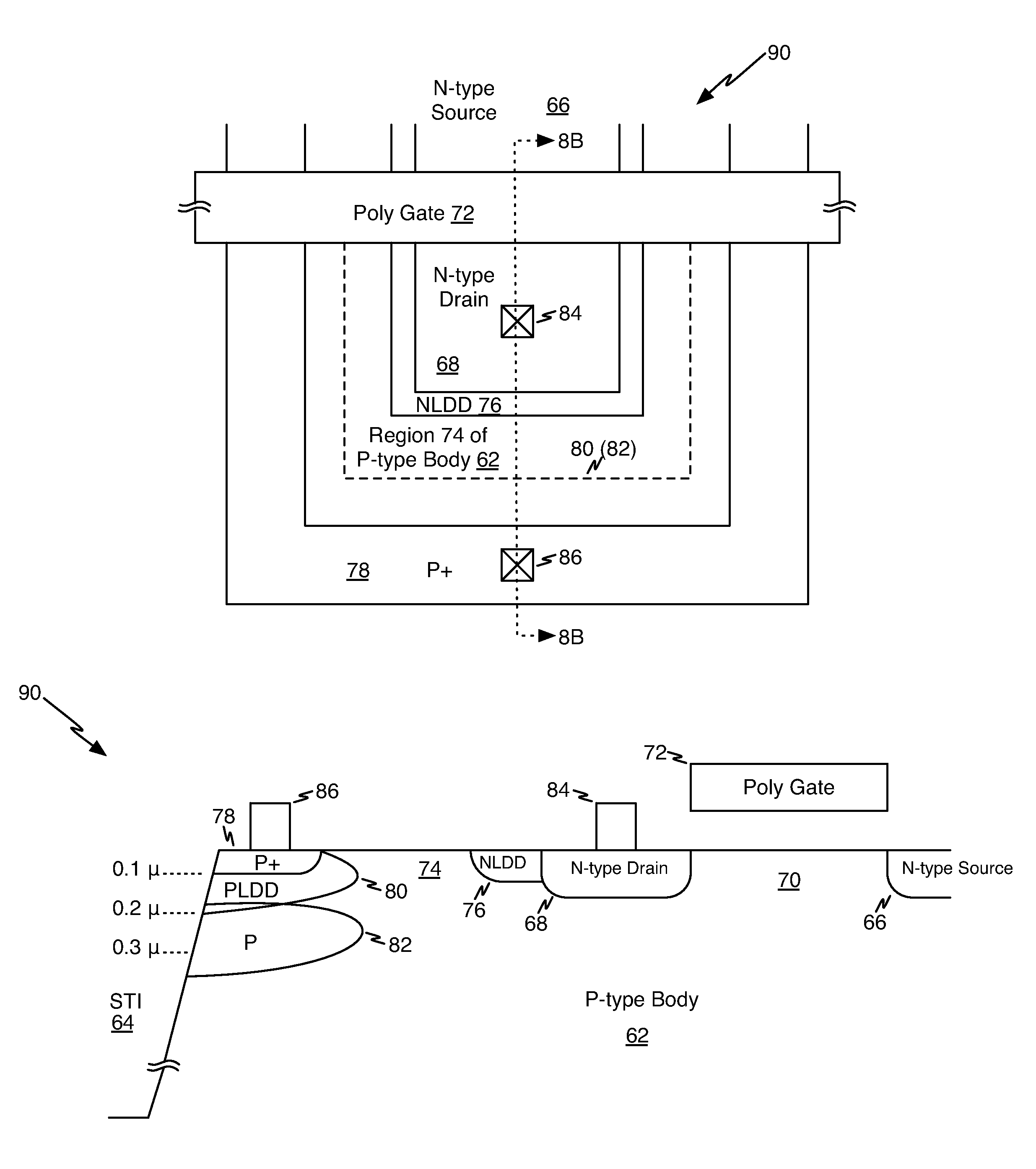
[0033]Referring now to FIGS. 3A, 3B, and 3C, the diagrams depict an illustrative embodiment of the present invention. According to this aspect of the present invention, the source and drain nodes of the NMOS transistor are electrically isolated from the trench sidewall by a lateral diode. This diode is junction engineered to provide isolation after exposure to ionizing radiation while maintaining the full junction breakdown performance of the original radiation-sensitive layout.

[0034]FIG. 3A is a three-dimensional drawing of the structure of a transistor 20 fabricated according to one aspect of the present invention. FIG. 3B is a cross-sectional view of the drain side of transistor 20 taken in a direction parallel to the channel. FIG....


PUM


Abstract

A radiation-hardened transistor is formed in a p-type body. An active region is disposed within the p-type body and has a perimeter defined by a shallow-trench isolation region filled with a dielectric material. Spaced-apart source and drain regions are disposed in the active region, forming a channel therebetween. A polysilicon gate is disposed above, aligned with, and insulated from the channel region. A p-type isolation ring is disposed in the p-type body separating outer edges of at least one of the source and drain regions from the perimeter of the active region. A body contact is disposed in the p-type isolation ring.

Description

CROSS REFERENCE TO RELATED APPLICATIONS[0001]This application is a continuation-in-part of prior co-pending U.S. patent application Ser. No. 13 / 895,554, filed May 16, 2013, and entitled “TID Hardened MOS Transistors and Fabrication Process,” which claims the priority benefit of U.S. Provisional Patent Application No. 61 / 651,689, filed May 25, 2012, and entitled “TID Hardened MOS Transistors and Fabrication Process.” This application also claims the benefits of U.S. Provisional Patent Application No. 61 / 772,476, filed Mar. 4, 2013, and entitled “TID Hardened and Single Event Transient Single Event Latchup Resistant MOS Transistors and Fabrication Process” all of which are incorporated herein by reference in their entirety.BACKGROUND OF THE INVENTION[0002]1. Field of the Invention[0003]The present invention relates to semiconductor technology, and specifically to MOS technology. More particularly, the present invention relates to radiation hardened MOS transistors and to methods for f...

Claims


Application Information

Patent Timeline
Patent Type & Authority Patents(United States)
IPC IPC(8): H01L29/78H01L29/06H01L29/10H01L29/08
CPCH01L29/78H01L29/0638H01L29/0642H01L29/0646H01L29/1083H01L29/0615H01L29/0847H01L29/0692H01L29/1087
Inventor SCHMID, BEN A.DHAOUI, FETHIMCCOLLUM, JOHN
Owner MICROSEMI SOC
Why Eureka
Try Eureka