Semiconductor driver circuit and power conversion device

a technology of driver circuit and power conversion device, which is applied in the direction of pulse generator, pulse technique, instruments, etc., to achieve the effects of improving power device performance, improving infrastructural power efficiency, and reducing environmental burden

Inactive Publication Date: 2015-08-04
HITACHI LTD
View PDF15 Cites 22 Cited by
  • Summary
  • Abstract
  • Description
  • Claims
  • Application Information

AI Technical Summary

Benefits of technology

[0004]In such large social trends as global environment conservation, the significance of electronics business whose environmental burden is reduced has been increased. Above all, a power device is used for inverters of a railroad vehicle and hybrid / electric vehicles, an inverter of an air conditioner, a power supply of consumer equipment such as a personal computer, and others, and improvement in a performance of the power device largely contributes to improvement in power efficiencies of an infrastructural system and consumer equipment. The improvement in the power efficiencies means reduction of energy resources required for operating systems, in other words, means emission reduction of carbon dioxide, that is, the reduction of the environmental burden. Accordingly, research and development for improving the performance of the power device have been actively performed.
[0005]Generally, a material of the power device is silicon (Si) as similar to that of a large scale integrated circuit (LSI). In a power conversion device (such as an inverter) using this Si power device, development for achieving such characteristics as low ON resistance (Ron), high current density, and high breakdown voltage has been actively performed by optimizing device structures of a diode and a switch element and a profile of an impurity concentration in order to reduce energy loss caused in the inverter or others. Also, in recent years, a chemical compound semiconductor such as silicon carbide (SiC) and gallium nitride (GaN) whose band gap is larger than that of silicon has been focused as the material of the power device. Since the chemical compound semiconductor has the large band gap, it has a breakdown voltage which is 10 times a breakdown voltage of silicon or higher. Therefore, a chemical compound device has a thinner film thickness than that of a Si device so as to drastically decrease the resistance value (Ron) upon the conduction. As a result, so-called conduction loss (Ron·i2) which is expressed by a product of the resistance value (Ron) and a conduction current (i) can be reduced so as to largely contribute to the improvement in the power efficiencies. In the focus on such a feature, development for a diode and a switch element using the chemical compound material has been actively performed.
[0008]That is, since the threshold shifts toward the negative side, short-circuit current loss due to so-called false firing is caused in the inverter device in some cases. This false firing is caused in a case, for example, as illustrated in FIG. 15 that the upper arm is turned from the OFF state to the ON state (for example, VGSU: −5 V to +15 V) in a condition in which the lower arm is the OFF state (for example, VGSD=−5 V). In this case, due to rapid increase in a drain voltage VDSD of the lower arm, a discharge / charge current is flown through a capacity between the gate and the drain of the switch element of the lower arm, and, as a result, the gate / source voltage VGSD of the switch element of the lower arm increases from a voltage level of the OFF state. And, if this voltage level exceeds a threshold of the switch element, the switch element of the lower arm whose state should be normally the OFF state is erroneously turned ON. Such phenomena that a switch to be normally OFF is erroneously turned ON are referred to as false firing. The false firing can be also caused in a case of using the Si MOSFET as the switch element of the lower arm. However, particularly in the case of using the Si CMOS, the false firing is easier to occur because the threshold shifts toward the negative side due to the continuous application of the negative voltage to the gate in the OFF period. Further, the longer the time of the application of the negative voltage is, the larger a degree of this threshold shift is, and therefore, the longer the time of the application of the negative voltage is, the further the false firing is easier to occur.
[0015]The effects obtained by typical aspects of the present invention disclosed in the present application will be briefly described below. In a power conversion device provided with a power semiconductor device and a semiconductor driver circuit for driving the power semiconductor device, the false firing can be prevented, and the improvement in the reliability can be achieved.

Problems solved by technology

However, regarding the SiCMOS, a problem that a threshold voltage is varied by the continuous conducting operation has been reported as described in Non-Patent Documents 1 to 3. FIG. 14 illustrates an outline of “drain current—gate current characteristics” obtained when the threshold voltage is varied.

Method used


Image

  • Semiconductor driver circuit and power conversion device
  • Semiconductor driver circuit and power conversion device
  • Semiconductor driver circuit and power conversion device

Examples


first embodiment

[0038](First Embodiment)

[0039]>

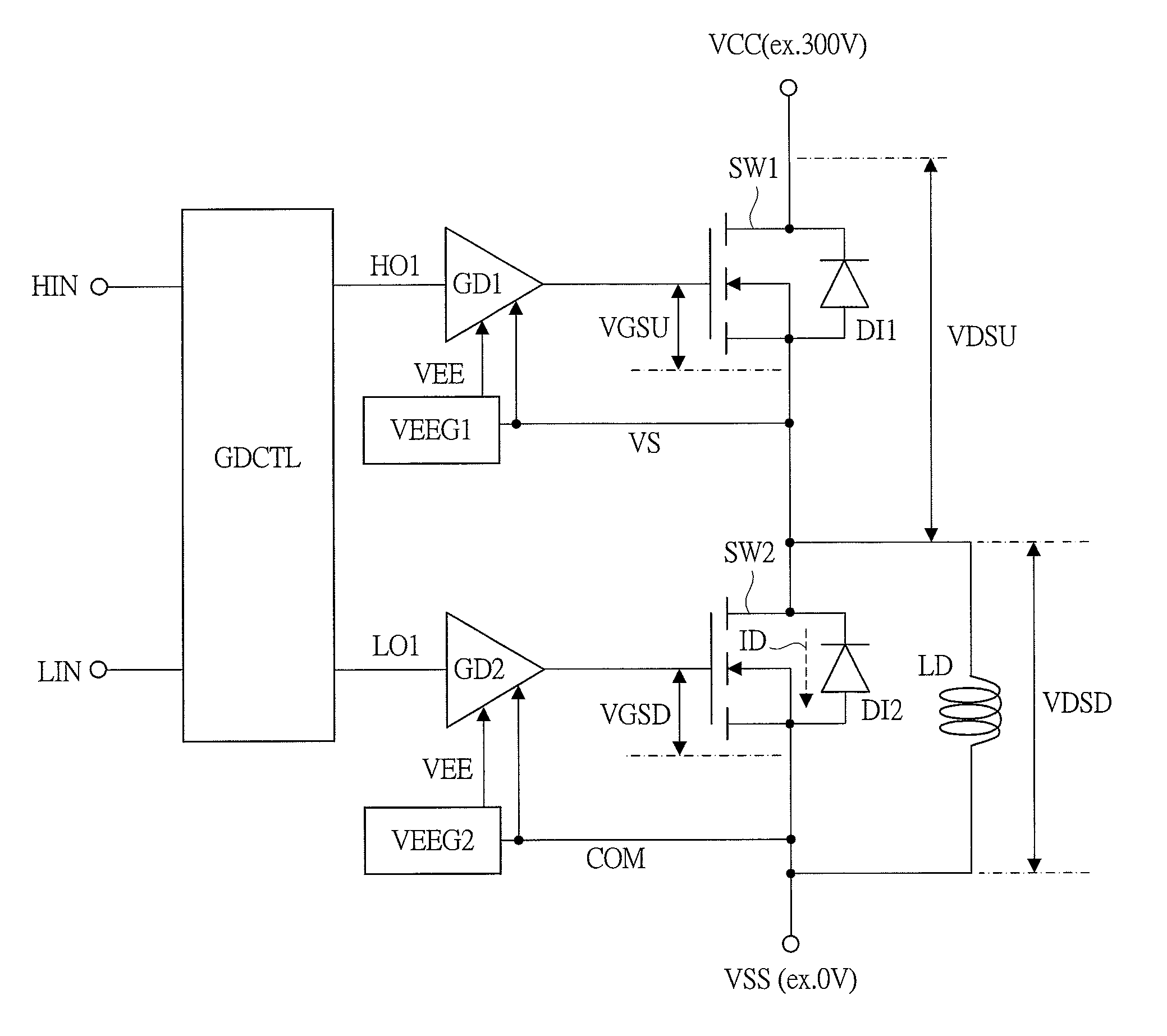
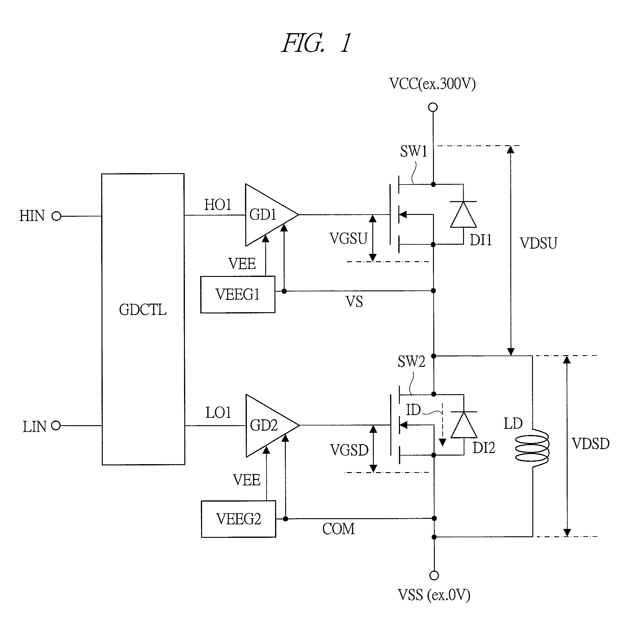
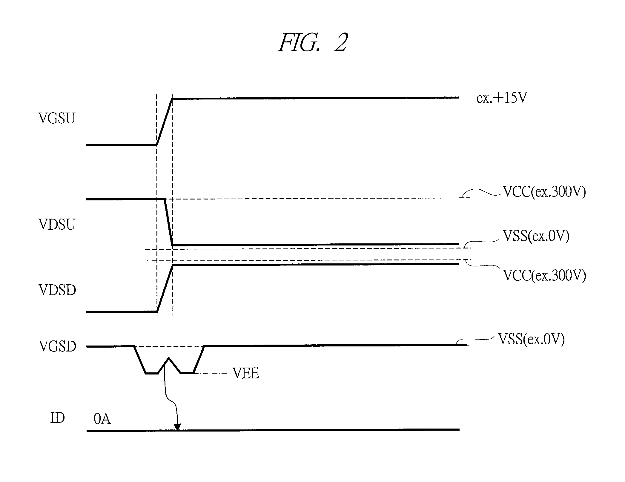
[0040]FIG. 1 is a schematic diagram illustrating a configuration example of a principal part of a power conversion device according to a first embodiment of the present invention. Here, the power conversion device as illustrated in FIG. 1 is a half bridge circuit. The half bridge circuit is appropriately used for such various purposes as a part of a power supply device of a DC / DC conversion circuit or others, as a part of a power supply device of a DC / AC conversion circuit or others by expansion into a full bridge circuit, a three phase inverter circuit, or others, and as a part of a motor control device. The half bridge circuit of FIG. 1 is provided with: a gate driver control circuit GDCTL; an upper-arm side switch element SW1 and a lower-arm side switch element SW2; free wheel diodes DI1 and DI2 corresponding to the respective switch elements SW1 and SW2; gate driver circuits GD1 and GD2 corresponding thereto; and negative-potential generating circu...

second embodiment

[0070](Second Embodiment)

[0071]>

[0072]FIG. 7 is a schematic diagram illustrating a configuration example of a principal part of a power conversion device according to a second embodiment of the present invention. The power conversion device as illustrated in FIG. 7 has a configuration with additional current detecting resistors Rs1 and Rs2 and current detecting circuits ISEN1 and ISEN2 in comparison to the configuration example of FIG. 1. The Rs1 is inserted between the source of the upper-arm side switch element SW1 and the drain of the lower-arm side switch element SW2, and the Rs2 is inserted between the source of the SW2 and the ground power supply voltage VSS. The ISEN1 detects a voltage between both ends of the Rs1 and outputs a detected voltage signal CM1, and the ISEN2 detects a voltage between both ends of the Rs2 and outputs a detected voltage signal CM2. The CM1 and CM2 are used in the negative potential generating circuit VEEG1 and VEEG2, respectively.

[0073]FIG. 8 is a s...

third embodiment

[0075](Third Embodiment)

[0076]>

[0077]FIG. 9 is a schematic diagram illustrating one example of a configuration of a power conversion device according to a third embodiment of the present invention. The power conversion device illustrated in FIG. 9 is obtained by, for example, applying the method of the first embodiment to so-called three-phase inverter device. In FIG. 9, each of SW1u, SW1v, SW1w, SW2u, SW2v, and SW2w is a switch element using an n-channel type SiCMOS, and respective free wheel diodes D1u, D1v, D1w, D2u, D2v, D2w are connected to between the respective sources and drains. The SW1u, SW1v, and SW1w are arranged on the upper-arm side while the SW2u, SW2v, and SW2w are arranged on the lower-arm side, and the SW1u and SW2u are for a U phase, the SW1v and SW2v are for a V phase, and the SW1w and SW2w are for a W phase.

[0078]GD1u, GD1v, GD1w, GD2u, GD2v, and GD2w are gate driver circuits as illustrated in FIG. 1, and drive the SW1u, SW1v, SW1w, SW2u, SW2v, and SW2w, respect...


PUM


Abstract

In a power conversion device provided with a power semiconductor device and a semiconductor driver circuit for driving the power semiconductor device, false firing can be prevented, and improvement in reliability can be achieved. The power conversion device is provided with: a first switch element inserted between a power supply voltage and an output node; a second switch element inserted between a ground power supply voltage and the output node; and a gate driver circuit for controlling turning ON / OFF of the second switch element. When the second switch element is controlled to be turned OFF, the gate driver circuit drives a gate-source voltage at, for example, a level of 0 V. However, when the first switch element is shifted from an OFF state to an ON state at a first timing in a state that the gate-source voltage is driven at, for example, the level of 0 V, the gate driver circuit temporarily applies a level of a negative voltage as the gate-source voltage during a first period which crosses over the first timing.

Description

CROSS-REFERENCE TO RELATED APPLICATION[0001]The present application claims priority from Japanese Patent Application No. 2012-086686 filed on Apr. 5, 2012, the content of which is hereby incorporated by reference into this application.TECHNICAL FIELD OF THE INVENTION[0002]The present invention relates to a semiconductor driver circuit and a power conversion device, and relates to a technique effectively applied to, for example, a power conversion device provided with a power semiconductor device using silicon, silicon carbide material, or others and a semiconductor driver circuit for driving the power semiconductor device.BACKGROUND OF THE INVENTION[0003]For example, Japanese Patent Application Laid-Open Publication No. 2000-333441 (Patent Document 1) describes a configuration in which, in order to shorten a mirror time of an insulating-gate type semiconductor element and shorten a dead time of a PWM inverter provided with the semiconductor element, a series circuit including a capa...

Claims


Application Information

Patent Timeline
Patent Type & Authority Patents(United States)
IPC IPC(8): G05F3/16H03K17/94H02M3/158H03K17/16H03K17/06
CPCH03K17/94H02M3/158H03K17/162H03K2017/066H01L2924/181H01L2224/0603H01L2224/48247H01L2224/4903H01L2924/13091H01L2924/00012H01L2924/00
Inventor AKIYAMA, SATORU
Owner HITACHI LTD
Why Eureka
Try Eureka