Method and system for detecting defects of transparent substrate

a technology of transparent substrates and defects, applied in the field of methods, can solve the problems of increasing the difficulty of image processing for defects detection and categorizing, misclassification of particles as real defects, and high cost and large size, and achieves the effects of low cost, long life and convenient heat dissipation

Inactive Publication Date: 2015-08-18
SAINT-GOBAIN GLASS FRANCE
View PDF22 Cites 6 Cited by
  • Summary
  • Abstract
  • Description
  • Claims
  • Application Information

AI Technical Summary

Benefits of technology

[0008]An object of the present invention is to provide an optical method and optical system for inspecting defects of a transparent substrate. The method and system of the present invention is capable of providing images of a plurality of inspection channels by sharing not only an imaging component but also an illumination component. By way of controlling a plurality of illumination components illuminate the substrate alternately, interference of multiple inspection channels is eliminated. The method and system described by the present invention is capable of discriminating real defects from fake defects which enable inspected substrate is free of cleaning.
[0011]Defect detection configuration of the present invention is compact and low cost by sharing at least part of illumination component and imaging components with a plurality of different inspection channel. Furthermore, since illumination component work in a pulse mode which facilitates heat dissipation, the illumination component may have a long lifetime and provide higher brightness. (In addition, since inspection zone of multiple inspection channels is confined in narrow strip, influence of substrate flattering during conveying of substrate is significantly reduced.) Moreover, in the present invention, by way of controlling a plurality of illumination components to illuminate the substrate alternately via trigger controlling, interference of multiple inspection channels is eliminated.

Problems solved by technology

Disadvantages of this system are high cost and large size due to each detection module will have a full set of illumination component, sensing component and image processing component.
As a result, difficulty of image processing for defects detection and categorization will be increased.
Usually, washing process of substrate is required before inspection of defects since foreign particles such as dust on surface of the substrate may result in misclassification of the particles misclassified as real defects.
It will undoubtedly increase fake defects rate of inspection (i.e. the probability of categorizing fake defects as real defects) and consequently increase waste of qualified product.
However, a washing machine is typically expensive in terms of cost of the equipment and electric power consumption.
On the other hand, washing process sometimes is not feasible or has negative influence on the substrate.
Another example is glass substrates of flat planes display module, which have a thickness of around 0.7 mm and are likely to break during washing process due to small thickness.
A further example is that water mark on the substrate is not acceptable for some applications.

Method used


Image

  • Method and system for detecting defects of transparent substrate
  • Method and system for detecting defects of transparent substrate
  • Method and system for detecting defects of transparent substrate

Examples


first embodiment

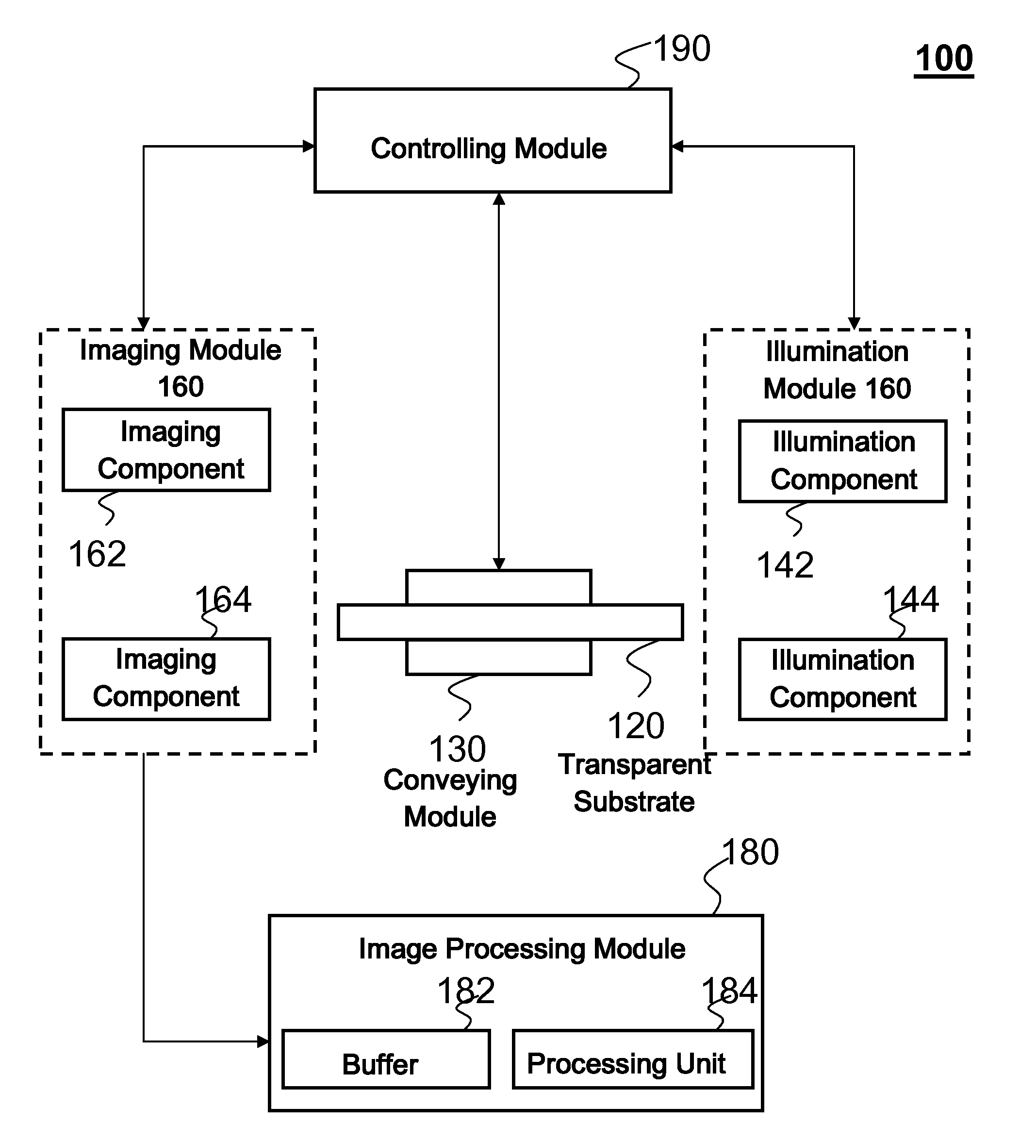
[0022]FIG. 1 shows a system 100 for detecting defects of a transparent substrate 120 according to the present invention. The defect detection system 100 comprises a transport module 130, an illumination module 140, an imaging module 160, an image processing module 180 and a controlling module 190. In order to remove the influence of environment light, the whole system 100 may be covered with a black cover (not shown in FIG. 1).

[0023]In the first embodiment, the transparent substrate 120 may be glass, plastic, or any other transparent material, such as glass ribbon on float line, raw glass panel, glass substrate of photovoltaic module and glass substrate of flat panel display device. The substrate 120 is not limited to the form of a sheet having substantially parallel surfaces, but can be extended to the form of a cylinder curved in a plane vertical to transporting direction of the substrate. Unless otherwise specified, as used therein, the term “two opposite sides of the substrate” ...

third embodiment

[0045]In addition, for example, the detection system of the present invention may use one imaging component 162 and a plurality of (three in the embodiment shown in FIG. 6) illumination components 142, 144, 746. As illustrated in FIG. 6, the illumination components 142 and 746 are located on the same side of the substrate 120 as the imaging component 162, while the illumination component 144 is located on the other side of the substrate 120. Here, the illumination components 142 and 746 provide dark field reflection illumination to the substrate 120 relative to imaging component 162 at different illumination angles, while the illumination component 144 provides bright field transmission illumination to the substrate 120 relative to imaging component 162. The controlling module 190 performs controlling operation so that the illumination component 142 and illumination component 746 may switch on simultaneously or not simultaneously, but either of them is switched on simultaneously wit...

fourth embodiment

[0046]FIG. 7 illustrates a four-channel optical configuration according to the present invention. As shown in FIG. 7, the system 100 includes four detection channels, i.e., a first detection channel, a second detection channel, a third detection channel and a fourth detection channel.

[0047]The first detection channel may include a dichromic mirror 310 placed on one side of the substrate 120 and capable of transmitting a red color light to the substrate 120 and reflecting a blue color light, a dual color illumination component 148 placed on the one side of the substrate 120 and capable of emitting the red color light and the blue color light, and the first imaging component 162 placed on another opposite side of the substrate 120. The dual color illumination component 148 may be a dual color LED. In the first detection channel, the dual color illumination component 148 may emit the red color light to the dichromic mirror 310, the dichromic mirror 310 may transmit through the red colo...


PUM

PropertyMeasurementUnit
thicknessaaaaaaaaaa
transparentaaaaaaaaaa
transmissionaaaaaaaaaa

Abstract

A method and a system for detecting defects of a transparent substrate are provided. The system includes: a plurality of detection channels, each of which includes an illumination component for providing illumination to the substrate and an imaging component for scanning the substrate to provide image of the substrate; a transport module, for producing relative motion between the substrate and the illumination components and the imaging components included in the plurality of detection channels; and a controlling module, for controlling the illumination components and the imaging components included in the plurality of detection channels so that at least two illumination components of the illumination components included in the plurality of detection channels provide illumination to the substrate alternately, and the imaging component included in any of the plurality of detection channels scans the substrate when the illumination component included in that detection channel illuminates the substrate, wherein the imaging components included in at least two detection channels of the plurality of detections channels are the same imaging component. The method and system described by the present invention is capable of discriminating real defects from fake defects which enables substrate to be inspected with free of cleaning.

Description

CROSS-REFERENCE TO RELATED APPLICATIONS[0001]The present application is the U.S. National Stage of PCT / CN2010 / 072782, filed May 14, 2010, which in turn claims a priority to Chinese patent application No. 200910139054.5 filed on May 15, 2009. The content of all of the applications are incorporated herein by reference in their entirety.FIELD OF THE INVENTION[0002]The present invention generally relates to a method and system for detecting local defects of a substrate, and, more specifically, relates to an optical method and system for detecting local defects both within and on surface(s) of a transparent substrate.BACKGROUND OF THE INVENTION[0003]Defects inspection is very important in terms of quality control of substrate manufacturing. For example, In the filed of glass manufacture, various types of defects such as scratches, stains, tin pick-ups, chips in terms of surface defects, and bubbles, stones, knots in terms of internal defects, may be formed in glass substrate during the p...

Claims


Application Information

Patent Timeline
Patent Type & Authority Patents(United States)
IPC IPC(8): H04N7/18G01N21/896G06K9/00G01N21/88
CPCG01N21/896G01N21/88G06K9/00H04N7/18G01N2021/8825H04N7/181G06F18/00
Inventor ZHENG, YUANSCHWEITZER, JEAN-PHILIPPELIN, XIAOFENGCHEN, DAZHI
Owner SAINT-GOBAIN GLASS FRANCE
Why Eureka
Try Eureka