Sputtering method and sputtering apparatus

a sputtering apparatus and sputtering technology, applied in the direction of vacuum evaporation coating, semiconductor/solid-state device details, coatings, etc., can solve the problems of large concentration gradients, inability to provide large concentration gradients, and increase the size of the film forming apparatus, so as to save the time of transfer between the treatment vessels, the effect of reducing the size of the apparatus and improving throughpu

Active Publication Date: 2015-09-01
TOKYO ELECTRON LTD
View PDF13 Cites 0 Cited by
  • Summary
  • Abstract
  • Description
  • Claims
  • Application Information

AI Technical Summary

Benefits of technology

[0013]The present invention has been made considering such situations, and the objective is to provide a technique capable of easily forming an alloy layer containing an additive metal on a processing object to provide a concentration gradient in a thickness direction by sputtering in one treatment vessel. Another objective of the present invention is to provide a technique capable of easily controlling the concentration of the additive metal in the alloy layer when forming the alloy layer on the processing object by sputtering.
[0033]According to the present invention, the concentration of the additive metal in the alloy film on the processing object is changed by changing a parameter, such as the pressure in the treatment vessel, the electric power of the high-frequency for generating a plasma, or the electric power supplied to the metal target for drawing the plasma. Therefore, the films with different concentration of the additive metals, in other words, an alloy film with a concentration gradient of the additive metal in a thickness direction, may be formed in a shared treatment vessel. As a result, because it is not necessary to provide a plurality of treatment vessels for sputtering deposition, the size of the apparatus can be minimized, and the time to transfer between the treatment vessels can be saved, thereby the throughput can be improved. Further, since the database, in which the additive metal concentration intended to the alloy film is related to the parameter values, is prepared in advance, and the process is performed according to the parameter values read from the database, the additive metal concentration can easily be controlled, thereby the alloy film with a desired additive metal concentration can easily be obtained.

Problems solved by technology

For this reason, it is difficult to form the barrier film and the seed layer with a high uniformity in the depressed portion, thus the reliability against a barrier property, and the contactability of an interface with the seed layer is an issue.
However, because when forming a film by such a method, the control width of the gas is small because an organic liquid source is vaporized, thus a large concentration gradient can not be provided.
However, in such a case, it is necessary to use Cu alloys with different Mn concentrations as a metal target, which requires treatment vessels for the number of that targets for storing the target to process a substrate.
As a result, the size of the film forming apparatus increases and the substrate is needed to be transferred between the treatment vessels, which results in a decrease in throughput.
For this reason, it is bothersome work to replace the metal target by opening the vacuum container, which is required, and also, the vacuuming after the replacement work takes long time.

Method used


Image

  • Sputtering method and sputtering apparatus
  • Sputtering method and sputtering apparatus
  • Sputtering method and sputtering apparatus

Examples


Embodiment Construction

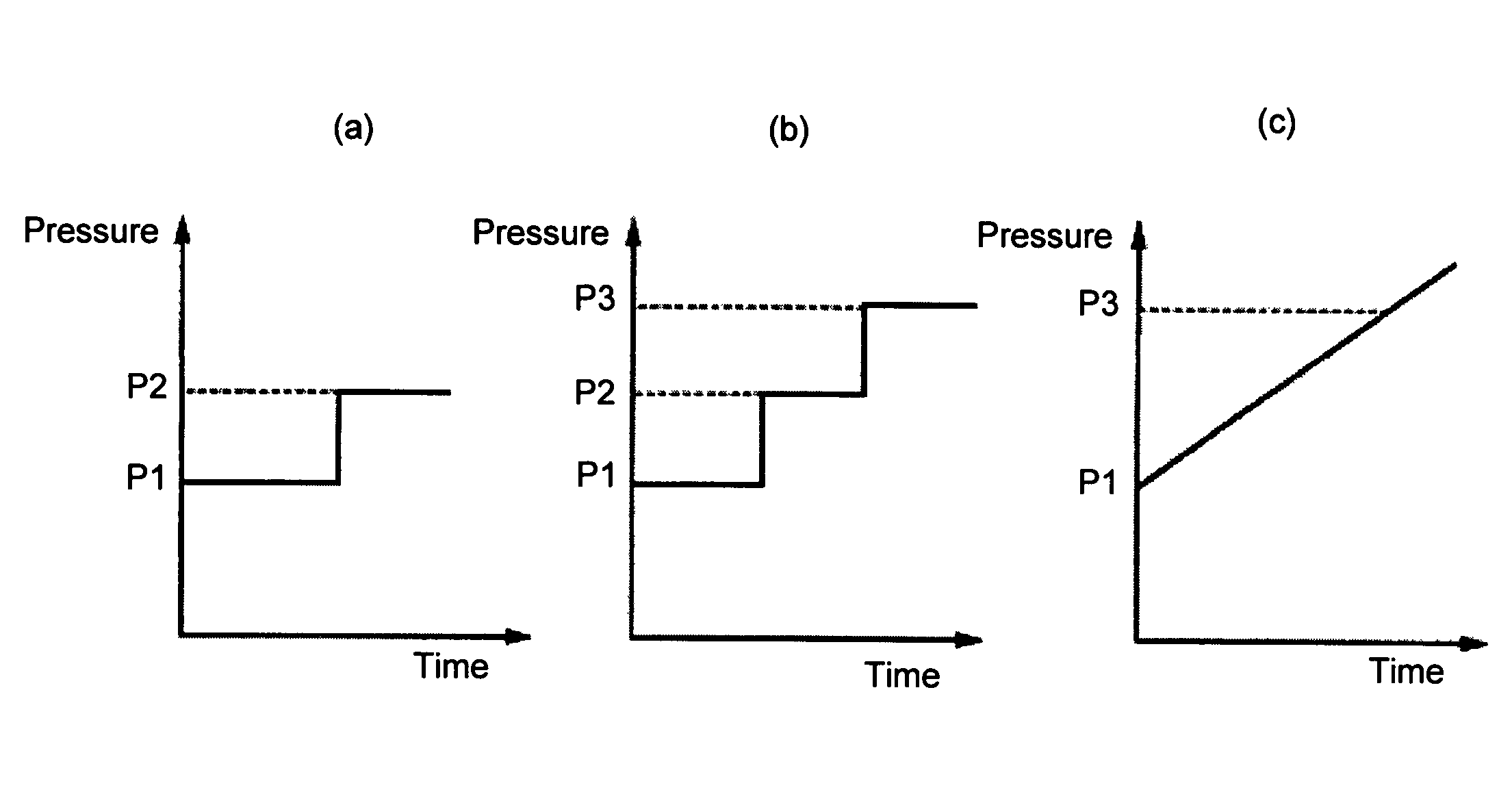
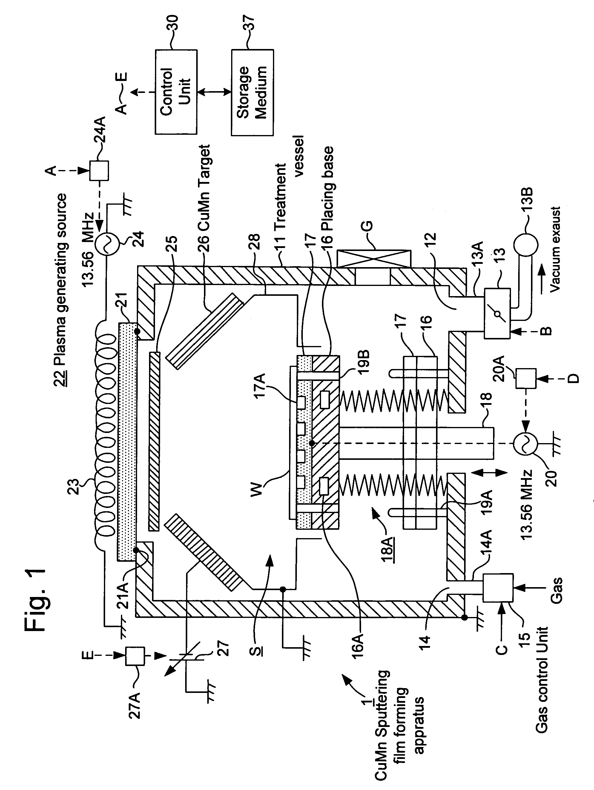
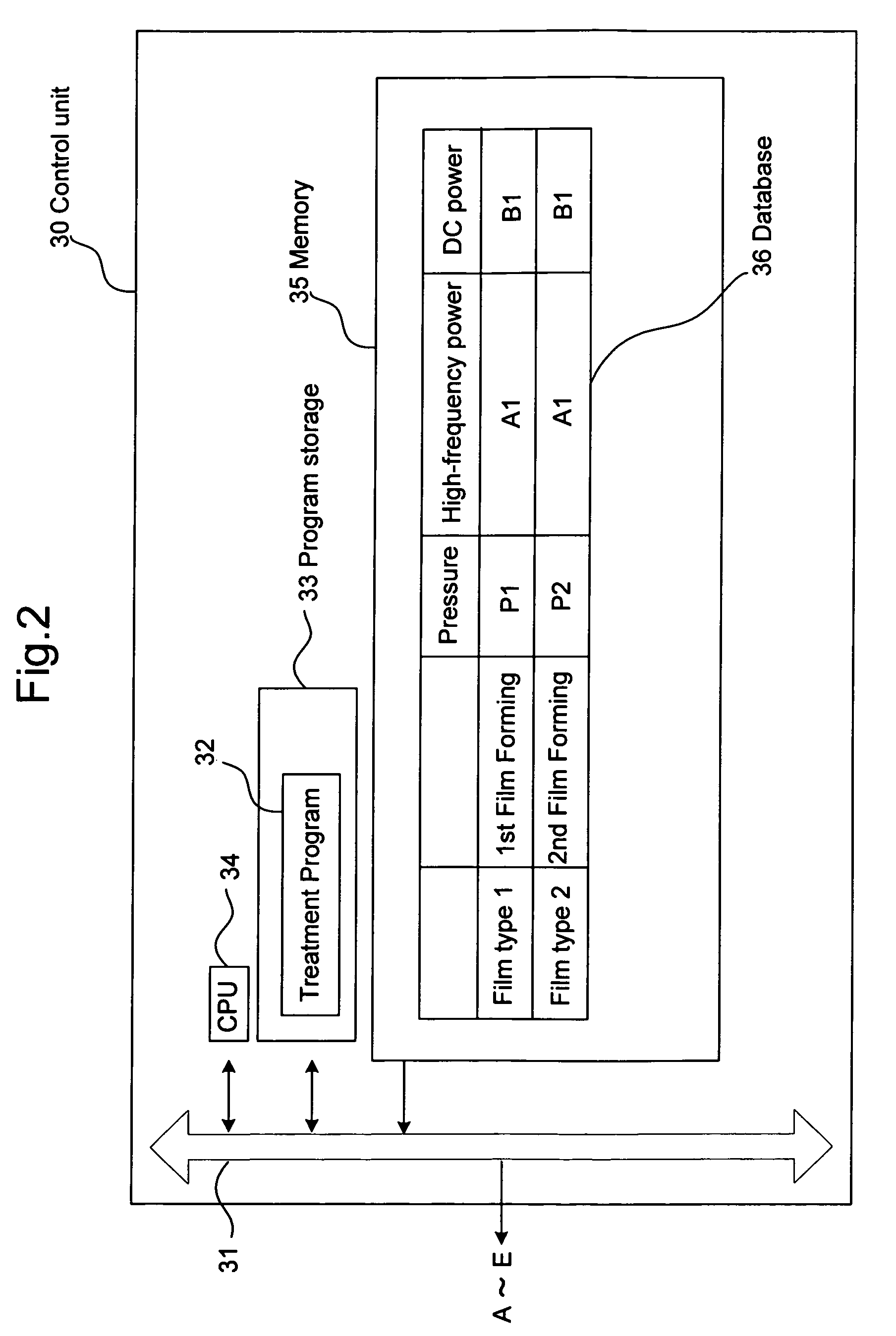
[0054]An embodiment, in which applying the sputtering film forming apparatus of the present invention to a CuMn sputtering film forming apparatus 1, is explained with reference to FIG. 1. This sputtering film forming apparatus 1 is called an ICP (Inductively Coupled Plasma) type plasma sputtering module, and has a treatment vessel 11, which formed in a cylindrical form with, for example, aluminum (Al) and so on. The treatment vessel 11 is grounded, and an exhaust outlet 12 is provided to the bottom. One end of an exhaust pipe 13A is connected to the exhaust outlet 12, and the other end of the exhaust pipe 13A is connected to a vacuum pump 13B through a throttle valve 13. With respect to the throttle valve 13, the degree of opening is adjusted according to a control signal transmitted from a control unit 30 described later and the treatment vessel 11 is evacuated, thereby a desired degree of vacuum is maintained. G in the figure is a gate valve to transfer a semiconductor wafer (here...


PUM

PropertyMeasurementUnit
pressureaaaaaaaaaa
pressureaaaaaaaaaa
electric poweraaaaaaaaaa

Abstract

The objective of the present invention is to provide a technique capable of easily forming an alloy layer containing an additive metal on an object to provide a concentration gradient in a thickness direction by sputtering in one treatment vessel. That is, the present invention can form a film with the desired concentration, and includes a first film forming process and a second film forming process that changes at least one of, the pressure in the treatment vessel, and the electric power so they are different from the first film forming process, so that the concentration of the additive metal is different from the concentration of the additive metal of the first alloy film.

Description

TECHNICAL FIELD[0001]The present invention relates to a sputtering method and a sputtering apparatus for depositing a main metal containing an additive metal on a treatment object.BACKGROUND OF THE INVENTION[0002]The multilayer wiring structure in a semiconductor device is formed by burying a metal wiring in an interlayer insulating film. A Cu (copper) is used as a material for this metal wiring because of low electromigration and low resistance, and a damascene process is commonly utilized as a forming process.[0003]In this damascene process, a trench for burying a wiring, which is to be arranged inside a layer, on an interlayer insulating film in a substrate, and a via hole for burying a connection wiring, which connects upper and lower wirings, are formed, and a Cu is buried on these depressed portions by a CVD or an electrolytic plating method. And, in order to favorably perform the burying of the Cu, it is necessary to form a very thin Cu seed layer along the inner face of the ...

Claims


Application Information

Patent Timeline
Patent Type & Authority Patents(United States)
IPC IPC(8): C23C14/34C23C14/18C23C14/02C23C14/54H01L21/285H01L21/768H01L23/532
CPCC23C14/185C23C14/027C23C14/345C23C14/544H01L21/2855H01L21/76844H01L21/76855H01L21/76873H01L21/76883H01L23/53238H01L2924/0002H01L2924/00H01L21/203H01L21/28
Inventor MAEKAWA, KAORUNAGAI, HIROYUKIHATANO, TATSUOSAKUMA, TAKASHI
Owner TOKYO ELECTRON LTD
Why Eureka
Try Eureka