
RFID tag, method for producing RFID tag, and mold

a technology of rfid tags and metal antennas, which is applied in the direction of loop antennas, antenna adaptation in movable bodies, instruments, etc., can solve the problems of user strangeness, metal antennas or ic chips which are included in rfid tags, and achieve high reliability

Inactive Publication Date: 2015-09-08
APIC YAMADA CORP
View PDF14 Cites 2 Cited by
  • Summary
  • Abstract
  • Description
  • Claims
  • Application Information

AI Technical Summary

Benefits of technology

The solution provides a reliable RFID tag that is comfortable against the skin, durable against washing and spinning, and securely attachable to fabrics without risk of damage from static electricity, ensuring effective wireless communication.

Problems solved by technology

However, the use of such an RFID tag on a fabric such as clothes often gives a user a feeling of strangeness due to contact between skin and the plastic film.
Moreover, the metal antenna or the IC chip which is included in the RFID tag may be destroyed because of the fragility under hard washing and spinning conditions such as those observed in the case of linen.

Method used


Image

  • RFID tag, method for producing RFID tag, and mold
  • RFID tag, method for producing RFID tag, and mold
  • RFID tag, method for producing RFID tag, and mold

Examples


first embodiment

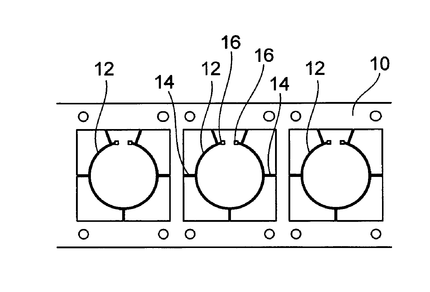
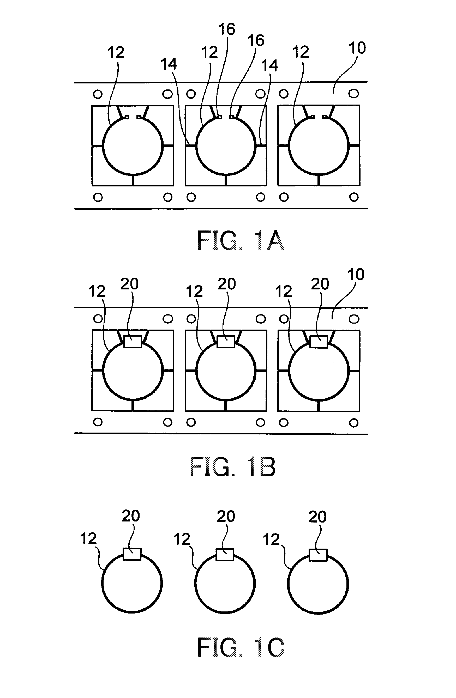
[0040]First of all, referring to FIGS. 1A to 1C and 2A to 2H, an RFID tag (Radio Frequency Identification Tag) and a method of manufacturing the RFID tag in the first embodiment of the present invention will be described. FIGS. 1A to 1C and 2A to 2H are manufacturing process diagrams of the RFID tag in this embodiment.

[0041]FIG. 1A illustrates a plan view of a metal strip 10 (not mounted on a semiconductor device) which is used for the RFID tag of this embodiment. The metal strip 10 is made of, for example a copper or ferrous sheet metal having a thickness of approximately 0.15 mm and is formed by stamping (pressing) or etching. The metal strip 10 includes loop antennas 12 (including micro loop antennas) each serving as an antenna of the RFID for wireless communications and terminals 16 configured to mount the semiconductor device, which is described later, to be electrically connected. Each loop antenna 12 is held by connecting portions 14. The configuration of each of the loop ant...

second embodiment

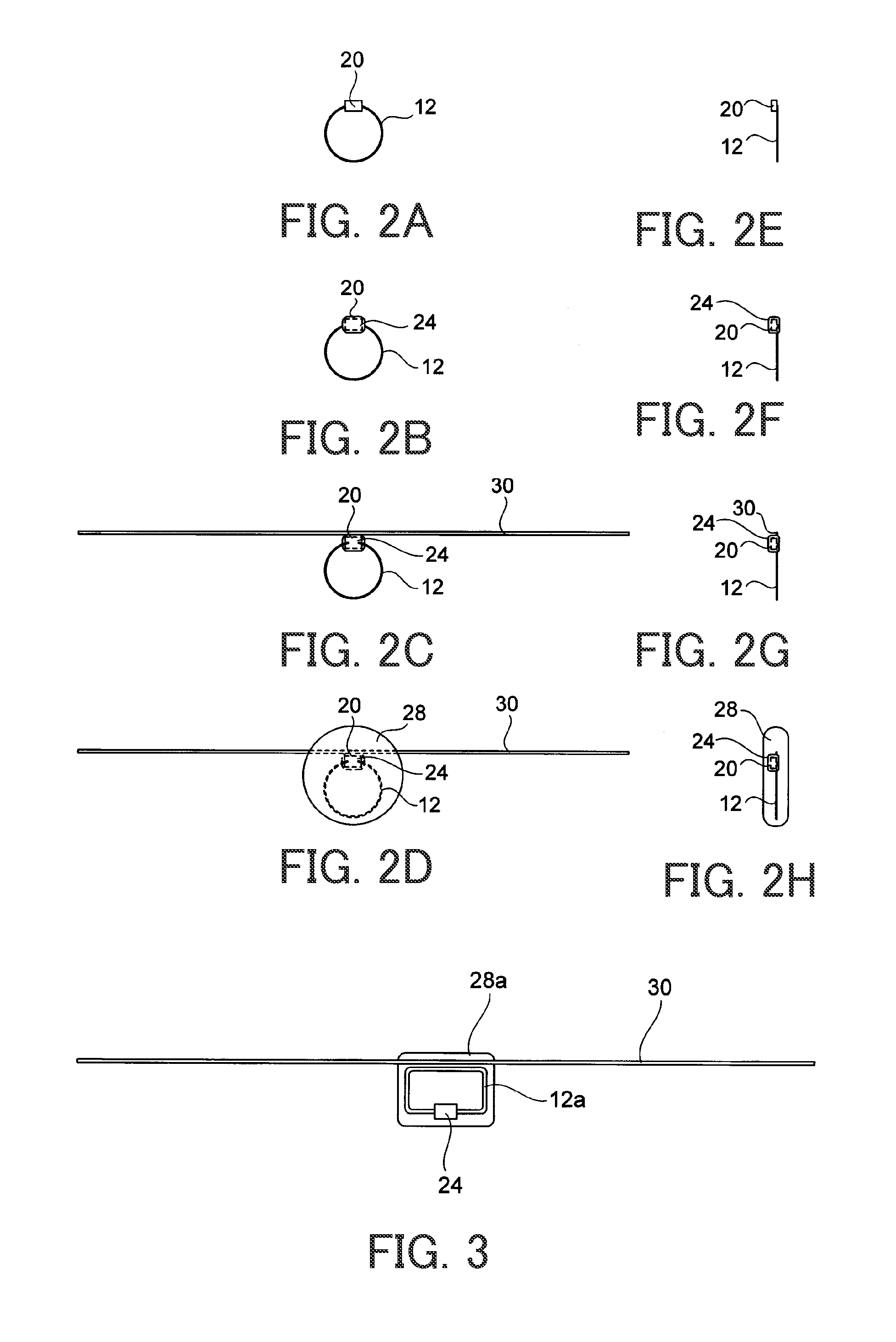
[0057]Next, an RFID tag in the second embodiment of the present invention will be described. FIGS. 4A to 4D are configuration diagrams of the RFID tag in this embodiment. FIG. 4A is a configuration diagram illustrating the inside of the RFID tag, FIG. 4B is a plan view of the RFID tag, FIG. 4C is a diagram illustrating a view as seen from the bottom of FIG. 4B (an elevation view), and FIG. 4D is a diagram illustrating a view as seen from the right side of FIG. 4B (a side view). As illustrated in FIGS. 4A to 4D, the RFID tag of this embodiment is configured such that the semiconductor device 20, as well as the main antenna 30 and the loop antenna 12, are directly and collectively sealed by using the resin 28, which is different from the RFID tag of the first embodiment in which the semiconductor device 20 is sealed with the resin 24 (the primary molding resin) and then collectively sealed with the resin 28 (the secondary molding resin).

[0058]FIG. 5 is a modification of the RFID tag i...

third embodiment

[0059]Next, an RFID tag in the third embodiment of the present invention will be described. FIGS. 6A to 6D are configuration diagrams of the RFID tag in this embodiment. FIG. 6A is a configuration diagram illustrating the inside of the RFID tag, FIG. 6B is a plan view of the RFID tag, FIG. 6C is a diagram illustrating a view as seen from the bottom of FIG. 6B (an elevation view), and FIG. 6D is a diagram illustrating a view as seen from the right side of FIG. 6B (a side view). The RFID tag of this embodiment is different from that of the second embodiment in that two through-holes 36 are formed on a resin 28b which collectively seals the main antenna 30, the loop antenna 12, and the semiconductor device 20. The formation of the through-holes on the resin 28b allows the through-holes 36 to be threaded. As a result, the RFID tag can be treated similarly to a fastening button, which makes it possible to easily attach the RFID tag to a fabric such as clothes. The main antenna 30 may be ...


PUM

PropertyMeasurementUnit
thicknessaaaaaaaaaa
melting pointaaaaaaaaaa
melting temperatureaaaaaaaaaa

Abstract

An RFID tag is provided which does not give a user a feeling of strangeness even when contacting his / her body and is firmly attachable to a fabric such as clothes. The RFID tag is for wireless communications and includes a main antenna 30 formed by a conductive fiber, a loop antenna 12 electrically coupled to the main antenna 30 without direct conductive connection, a semiconductor device 20 electrically connected to a terminal 16 of the loop antenna 12, and a resin 28 collectively sealing the main antenna 30, the loop antenna 12, and the semiconductor device 20.

Description

CLAIM FOR PRIORITY[0001]This application is a National Stage Entry of and claims priority under 35 U.S.C. §§365 and 371 to PCT application serial no. PCT / JP2012 / 005643, filed Sep. 6, 2012 and entitled “RFID TAG, METHOD FOR PRODUCING RFID TAG, AND DIE,” which in turn claims priority to Japanese patent application serial no. 2011-228944, filed Oct. 18, 2011 and entitled “Flip-Flop Circuit.” The entire contents of the aforementioned applications are herein expressly incorporated by reference.TECHNICAL FIELD[0002]The present invention relates to an RFID tag including a main antenna formed by a conductive fiber, a method of manufacturing the RFID tag, and a mold which is used for manufacturing the RFID tag.BACKGROUND[0003]Conventionally, an RFID tag has been generally configured by forming an antenna wire (a metal antenna) with a metal foil on a plastic film and mounting an IC chip on the antenna wire. However, the use of such an RFID tag on a fabric such as clothes often gives a user a ...

Claims


Application Information

Patent Timeline
Patent Type & Authority Patents(United States)
IPC IPC(8): G06K19/07G06K19/02G06K19/077H01Q1/27B29C45/14H01Q1/44H01Q1/22H01Q7/00
CPCG06K19/07783B29C45/14G06K19/027G06K19/0723G06K19/07724G06K19/07756G06K19/07794H01Q1/273H01Q1/44H01Q1/2225H01Q7/00Y10T29/41
Inventor ISHIDA, FUMIHITONISHIZAWA, MASAOKIDA, KENJIHIRANO, TADAHIKO
Owner APIC YAMADA CORP
Learn More