Light emitting diode device with luminescent material

a technology of light-emitting diodes and luminescent materials, which is applied in the direction of basic electric elements, chemistry apparatuses and processes, and light-emitting compositions. it can solve the problems of difficult practice, inconvenient handling of fluoride compounds, and insufficient light-emitting capacity, so as to improve the desired light-emitting performance, increase stability, and enhance the effect of light-emitting performan

Active Publication Date: 2015-09-15
LUMILEDS
View PDF13 Cites 3 Cited by
  • Summary
  • Abstract
  • Description
  • Claims
  • Application Information

AI Technical Summary

Benefits of technology

[0008]In addition, the invention has as an object to provide new LED devices with wavelength converting elements containing Mn4+-activated fluoride compounds which are less toxic and less sensitive towards humid environments.
[0011]The invention is based on the insight gained by the inventors that the sensitivity towards humid environments of Mn4+-activated fluoride compound with a garnet-type crystal structure is considerably less than the sensitivity towards humid environment of the known compounds described in WO 2009 / 012301. The described compounds do not have a garnet-type crystal structure. The inventors moreover believe that, in view of the chemically inert character of the new invented luminescent compounds, their toxicity is low as compared with similar known compounds disclosed in said patent publication. These properties of the luminescent compounds make their application in LED devices more attractive, both in the production and in the use of the devices.
[0019]A more preferred embodiment of the LED device according to the present invention is characterized in that in that the composition of the Mn4+-activated fluoride compound substantially answers the formula {Na3}[Al2-x-yMnxMgy](Li3)F12-dOd. The ranges of the indices are as described before. From experimental data, it was concluded that, within the described broader class of garnet-type compounds, this series of compounds is extremely stable. This stability makes the application of these compounds in LED devices very attractive, both in the production and in the use of the devices.
[0031]It is stressed that not only the invented Mn4+-activated fluoride compounds with garnet-type crystal structure in their pure form enhance the desired performance of the light in a LED device, but that also composite materials and mixed crystals of the invented compounds were found to do so. Composites are defined as consisting of two or more on finite scale distinguishable materials, e.g. core shell materials, composite ceramics or coated particles. A mixed crystal in contrast has a homogenous distribution of the constituting elements on atomic scale.
[0032]This invention therefore also pertains to composites of {A3}[B2-x-yMnxMgy](Li3)F12-dOd type garnets with oxide garnets A3B2(CO4)3 including but not limited to YAG (Y3Al5O12), Mg3Al2Si3O12 or Ca3Al2Si3O12. These composites are preferably oxide garnet coatings on {Na3}[Al2-x-yMnxMgy](Li3)F12-dOd type phosphor particles, or core shell materials, where the {Na3}[Al2-x-yMnxMgy](Li3)F12-dOd type is surrounded by an oxide garnet shell. The difference between a coating and a shell is mainly the relative amount of the respective materials, whereas a coating is less than 10% w / w of the total material, in a core shell material the shell may be 50% w / w or even more. The advantage of such coated or core shell materials are the increased stability with respect to humidity and the option to vary the refractive index of the phosphor. With increased stability it is also expected that toxicity will be further reduced.

Problems solved by technology

A first disadvantage to be mentioned concerns the fluoride compounds used in the wavelength converting elements, most of which are (less or more) toxic.
A second disadvantage pertains to the handling of these fluoride compounds, which in practice is not easy, due to their relatively high sensitivity towards humid environments.
Prolonged exposure of these materials to (humid) air causes formation of a thin water film on the surface of the material, leading to (surface) decomposition.
This disadvantageous property affects both the pure materials (causing short shelf times) and the LED devices in which they are applied (causing decrease of performance in time).

Method used


Image

  • Light emitting diode device with luminescent material
  • Light emitting diode device with luminescent material
  • Light emitting diode device with luminescent material

Examples


first embodiment

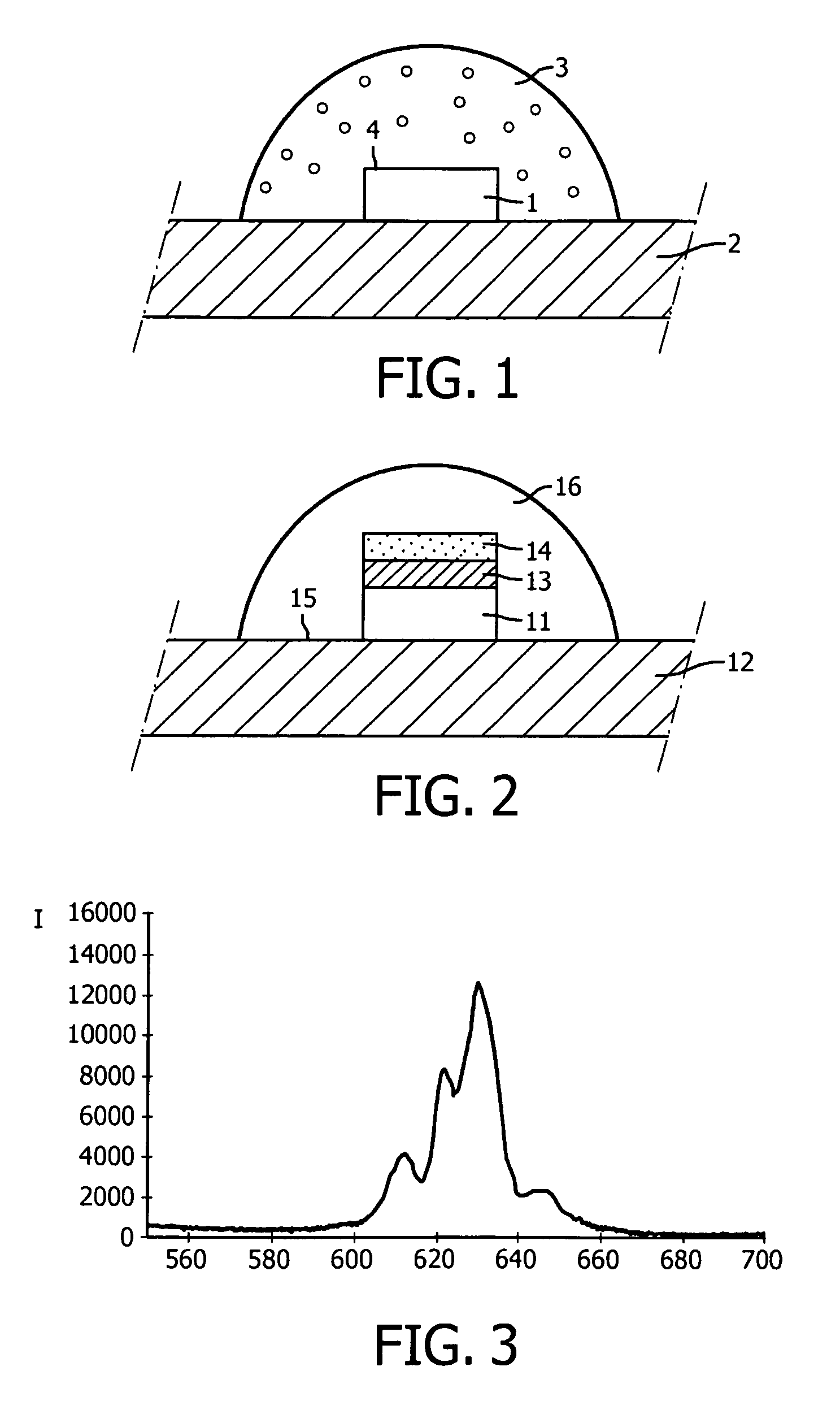
[0040]the present invention is schematically illustrated by FIG. 1. This Figure shows a cross-section of a LED device comprising a semiconductor light emitting diode (1), which is connected to a substrate (2), sometimes referred to as sub-mount. The diode (1) and substrate (2) are connected by means of appropriate connecting means, like solder or (metal-filled) adhesive.

[0041]The diode (1) is of the GaInN type, emitting during operation light having a wavelength of 450 nm. In the present embodiment, said light exits LED (1) via emitting surface (4). A wavelength converting element (3) formed as a convex lens shaped body is positioned adjacent to LED (1). This lens is largely made of a high temperature resistant silicone resin, in which grains are incorporated of a Mn4+-activated fluoride compound having a garnet-type crystal structure. Latter compound acts as a luminescent material in the lens. In the present embodiment said silicone resin contains 16 vol % {Na3}[Al1.94Mn0.03Mg0.03]...

second embodiment

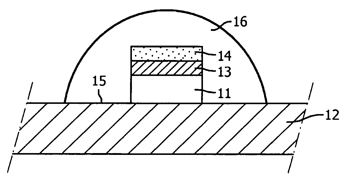
[0044]FIG. 2 depicts a schematic cross-section of the present invention designed as a white light generating LED device. This Figure shows a conventional blue or (near)UV generating light emitting diode (11), which is attached to a substrate (12) using solder bumps (not shown). Substrate (12) has metal contact pads on its surface to which LED (11) is electrically connected (not shown). By means of these solder pads, LED (11) can be connected to a power supply. In the present example, LED (11) is of the AlInGaN type and emits blue light having a peak wavelength of appr. 420-470 nm. It goes without saying that other semiconductor materials having other peak wavelengths can be used as well within the scope of the present invention.

[0045]Two wavelength converting elements formed as ceramic platelets (13) and (14) are positioned adjacent to LED (11). The platelets (13, 14) and LED (11) can mutually be affixed by means of an adhesive (like a high temperature resistant silicone material or...


PUM

PropertyMeasurementUnit
color temperatureaaaaaaaaaa
wavelengthaaaaaaaaaa
refractive indexaaaaaaaaaa

Abstract

The invention provides a light emitting diode device comprising a light emitting diode arranged on a substrate and a wavelength converting element. The wavelength converting element contains a luminescent material a Mn4+-activated fluoride compound having a garnet-type crystal structure. The Mn4+-activated fluoride compound preferably answers the general formula {A3}[B2-x-yMnxMgy](Li3)F12-dOd, in which formula A stands for at least one element selected from the series consisting of Na+ and K+ and B stands for at least one element selected from the series consisting of Al3+, B3+, Sc3+, Fe3+, Cr3+, Ti4+ and In3+, and in which formula x ranges between 0.02 and 0.2, y ranges between 0.0 (and incl. 0.0) and 0.4 and d ranges between 0 (and incl. 0) and 1. As the luminescent materials of the described type and structure have high stability and low sensitivity towards humid environments, they can advantageously be used as in wavelength conversion elements of LED devices.

Description

BACKGROUND OF THE INVENTION[0001]The invention relates to a light emitting diode device comprising a light emitting diode arranged on a substrate, and a wavelength converting element containing a Mn4+-activated fluoride compound. The invention also relates to a luminescent material as well as to a method for preparing such luminescent material.[0002]Light emitting diode devices (abbr. as LED devices) are widely known as new semiconductor light sources with promising lighting properties for future applications. These LED devices should eventually substitute many of the current light sources, like incandescent lamps. They are especially useful in display lights, warning lights, indicator lights and decoration lights.[0003]The color of the emitted light depends on the type of semiconductor material. LEDs produced from Group III-V alloys—such as GaN—are well-known for their ability to produce emission in the green to UV range of the electromagnetic spectrum. During the last decade, meth...

Claims


Application Information

Patent Timeline
Patent Type & Authority Patents(United States)
IPC IPC(8): C09K11/64C09K11/77H01L33/50C04B35/553
CPCC09K11/645C04B35/553C09K11/7774H01L33/502C04B2235/3201C04B2235/3203C04B2235/3206C04B2235/3217C04B2235/3224C04B2235/3241C04B2235/3262C04B2235/3272C04B2235/3286C04B2235/3409C04B2235/5292C04B2235/5436C04B2235/764H01L33/26H01L33/505H01L33/507
Inventor MEYER, JOERGWEILER, VOLKERSCHMIDT, JOSEF PETER
Owner LUMILEDS
Why Eureka
Try Eureka