Switch controls

a technology of switch control and control circuit, which is applied in the field of switch control circuits, can solve the problems of increasing the power loss of the bias network, decreasing resistance,

Active Publication Date: 2015-09-22
STMICROELECTRONICS INT NV
View PDF38 Cites 18 Cited by
  • Summary
  • Abstract
  • Description
  • Claims
  • Application Information

AI Technical Summary

Problems solved by technology

However, power loss scales as the inverse of the resistance, so decreasing resistance increases the power losses of the bias network.

Method used


Image

  • Switch controls
  • Switch controls
  • Switch controls

Examples


Embodiment Construction

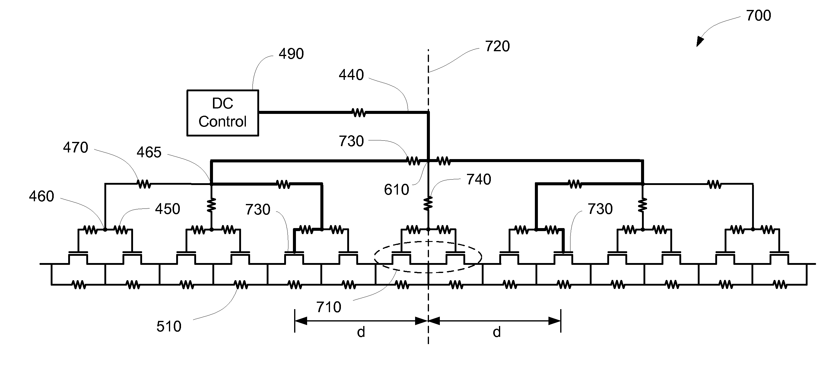
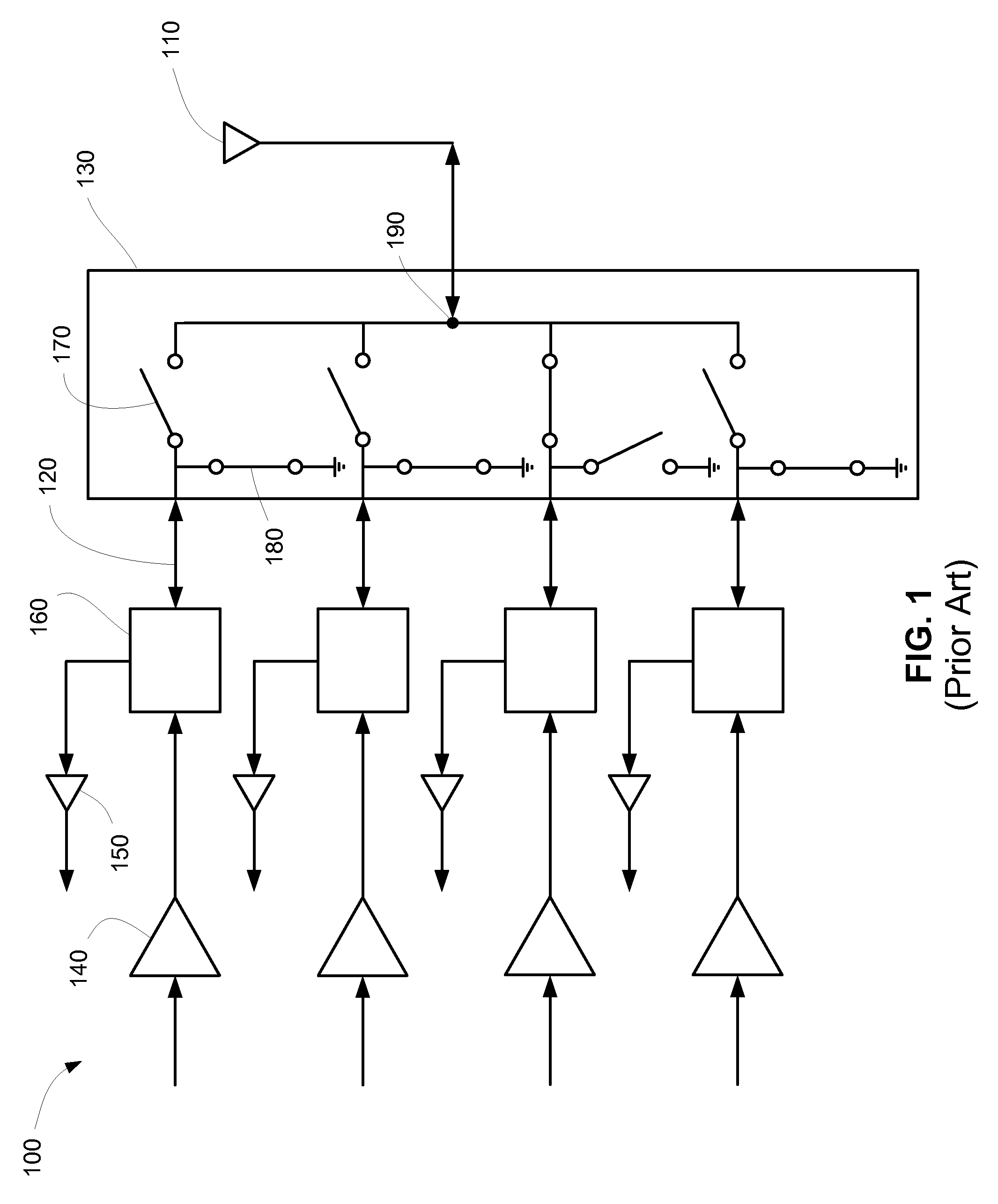
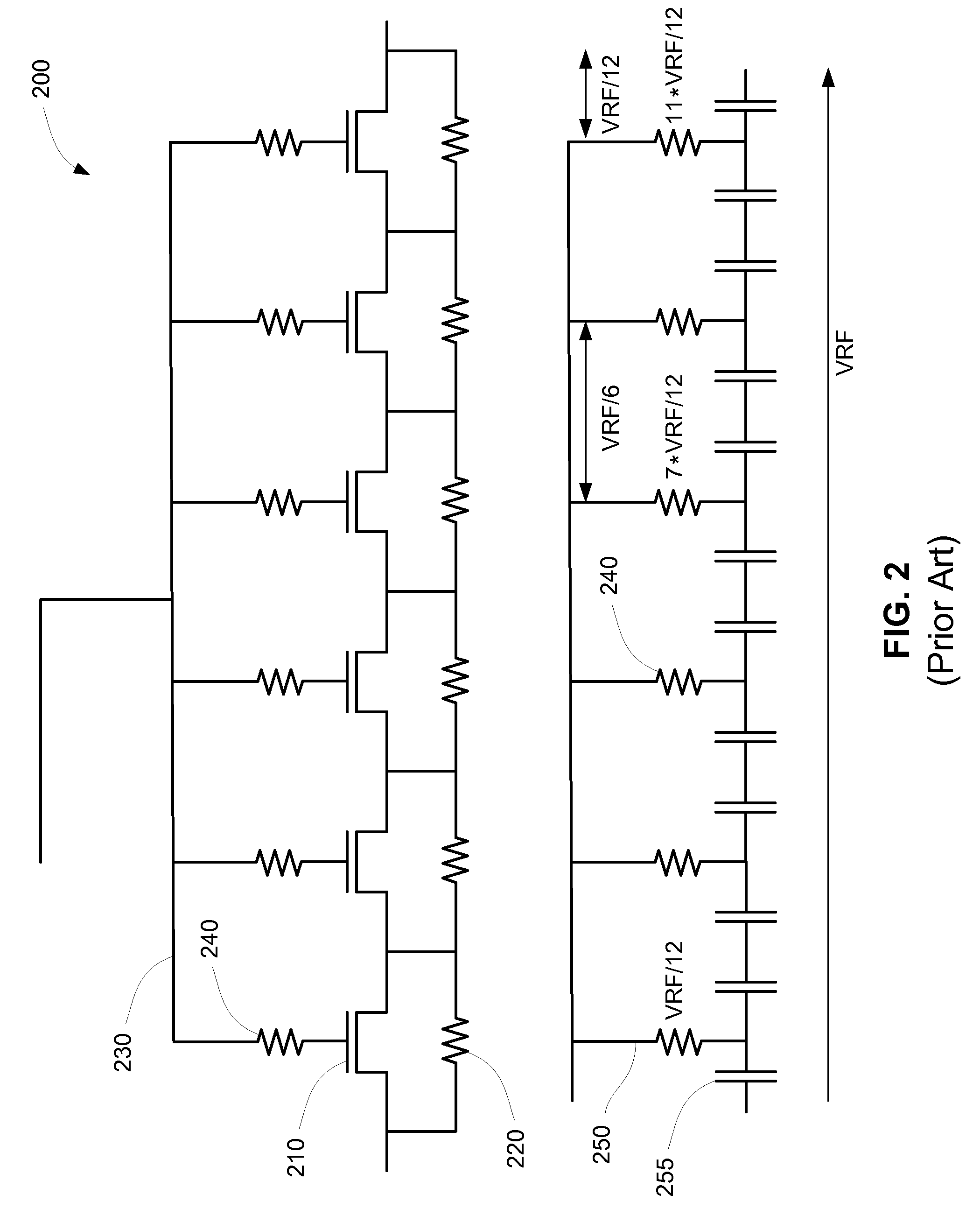
[0027]The present invention describes switches for use in RF applications such as phase shifters, step attenuators, and as serial 170 and parallel 180 switches in antenna switches 130, for example. The switches of the present invention provide a better balance of power losses in the OFF mode and switching times than the switches 200, 300 of the prior art. In some embodiments, switches of the present invention also provide second harmonic rejection by changing the single ended type RF signal between source and drain, as in the switches 200, 300 of FIGS. 2 and 3, to a differential one at gate level, due to the bias network symmetry.

[0028]FIG. 4 illustrates an exemplary switch 400 of the present invention. The switch 400 comprises an even number of transistors 410 arranged in series, where every two successive transistors 410 defines a pair 420 of transistors 410 such that the stack has half as many pairs 420 as transistors 410. The switch 400 also comprises a bias network 430 that con...


PUM


Abstract

Switches for use in RF devices are provided that offer a better balance of power losses and switching times than switches of the prior art. Switches of the present invention comprise a stack of transistors controlled a symmetric bias network. The stack of transistors includes an even number of transistors arranged in series, where every two successive transistors defines a pair. The bias network includes a symmetrically branching set of connections, where the gates of every pair of transistors are connected by a first connection having a first node, and two or more first nodes are connected by a second connection to a second node, and so forth. The symmetry of the bias network tends to reject even harmonics, and the rejection of even harmonics can be further enhanced by adding capacitors between the bias network and the stack of transistors at points of symmetry.

Description

BACKGROUND[0001]1. Field of Invention[0002]The present invention relates generally to RF circuits and more particularly to switches usable for activating and deactivating RF paths, including switching an antenna between multiple transit paths, and other applications.[0003]2. Related Art[0004]FIG. 1 illustrates a prior art RF circuit 100 coupled to an antenna 110. The circuit 100 comprises a number of transit paths 120 and an antenna switch 130 that couples the antenna 110 to the several transit paths 120. Each transit path 120 includes a power amplifier 140 and a receiver amplifier 150 alternately joined to the antenna switch 130 by a switch 160. Within the antenna switch 130, each transit path 120 is switchably coupled to the antenna 110 by a series switch 170 and optionally also switchably coupled to ground by a parallel switch 180.[0005]As shown in FIG. 1, when one transit path 120 is coupled to the antenna 110 (said to be in the ON mode), the series switch 170 for that transit p...

Claims


Application Information

Patent Timeline
Patent Type & Authority Patents(United States)
IPC IPC(8): H01Q13/00H01Q1/50H03K17/687H03D7/12H01Q13/02H04M1/725H04W24/00H04M1/724
CPCH03K17/687H01Q1/50H01Q13/02H03D7/125H04M1/72519H04W24/00H03K17/102H03K17/693H04B1/48H03K2217/0054H04B1/006H04B1/44H03K17/6874H04M1/724
Inventor CAM, HERVEVENEC, STEPHANIEDOS SANTOS, FILIPE
Owner STMICROELECTRONICS INT NV
Why Eureka
Try Eureka