Adjacent wordline disturb reduction using boron/indium implant

a technology of boron/indium implant and adjacent wordline, which is applied in the direction of electrical equipment, semiconductor devices, instruments, etc., can solve the problems of higher threshold voltage required to activate the row associated with the affected wordline, undesirable capacitance of the charge stored in the memory cell, etc., and achieve the effect of reducing parasitic current and facilitating reducing parasitic curren

Active Publication Date: 2015-10-06
INFINEON TECH LLC
View PDF11 Cites 0 Cited by
  • Summary
  • Abstract
  • Description
  • Claims
  • Application Information

AI Technical Summary

Benefits of technology

[0006]One aspect of the subject invention provides semiconductor devices having reduced parasitic currents in two or more conductive conduits. The conductive conduits may be formed from semiconductor material doped to allow passage of a current. The semiconductor devices contain two or more conductive conduits, a space formed between the conductive conduits and a charge storage layer capable of storing a charge, all formed over a semiconductor substrate. Boron, indium, or a combination of boron and indium is implanted into the space formed between the conductive conduits to facilitate reducing parasitic currents.

Problems solved by technology

As device dimensions shrink, charged stored in memory cells creates undesirable capacitance issues with neighboring elements within the memory device.
In particular, current flow in wordlines adjacent to programmed memory cells is often times disturbed resulting in a higher threshold voltage required to activate the row associated with the affected wordline.

Method used


Image

  • Adjacent wordline disturb reduction using boron/indium implant
  • Adjacent wordline disturb reduction using boron/indium implant
  • Adjacent wordline disturb reduction using boron/indium implant

Examples


Embodiment Construction

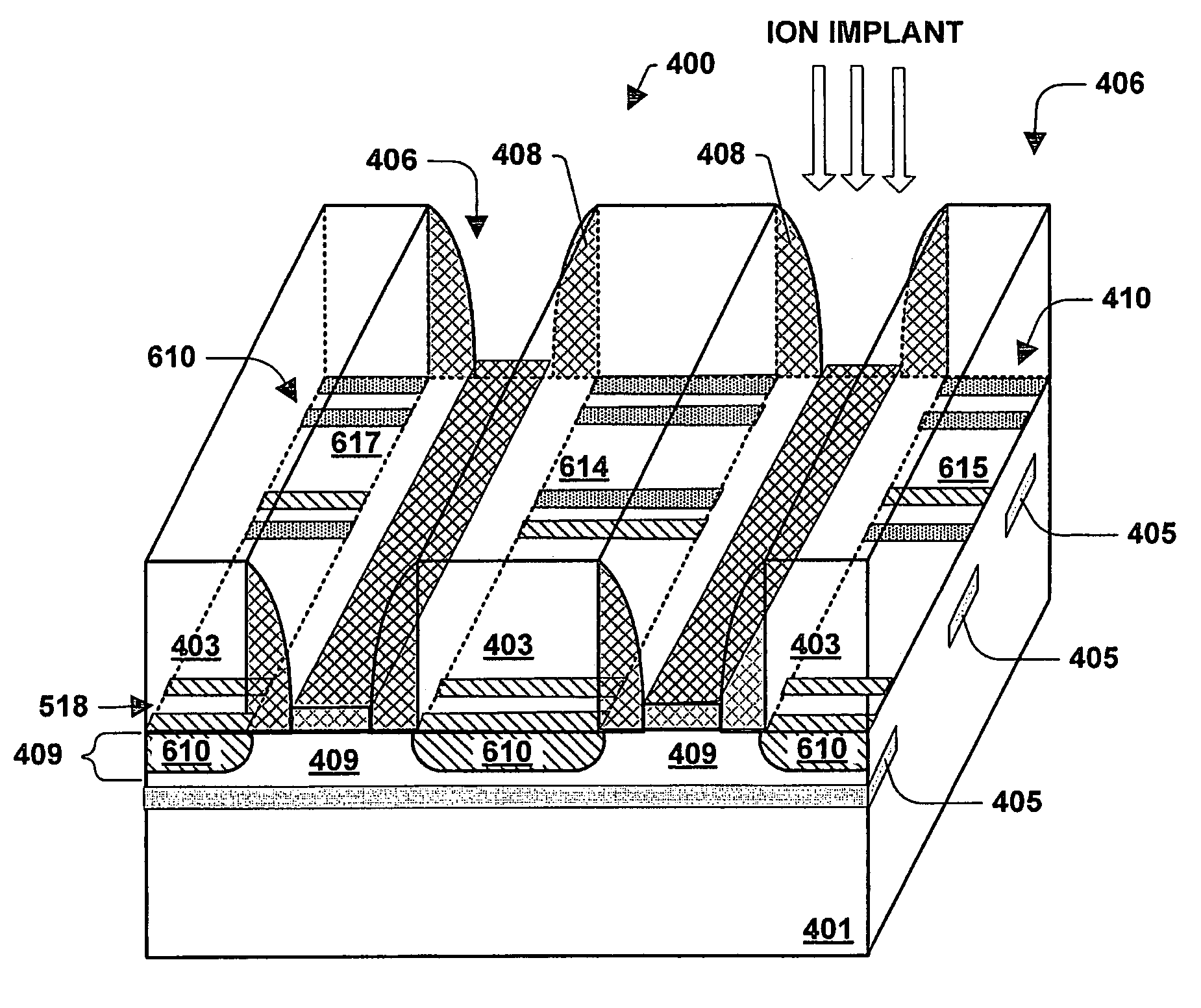
[0021]As semiconductor devices shrink in size, stored charge, for example, in the charge storage layer of a non-volatile memory device or in a capacitor of a volatile memory device, is located in close enough proximity to adjacent and other nearby device elements for capacitance to have a significant detrimental effect. Specifically, stored charge can cause an undesirable reduction in the current flow in adjacent conductive conduits formed on a semiconductor substrate. This reduction in current is often accompanied by current flowing along the edge of conductive conduits and even into the space between conduits, rather than through the center of the conduit. Conductive conduits are any conductive structure formed of material deposited on or over a semiconductor substrate. Conductive conduits, include, but are not limited to, wordlines in memory devices and other conductive pathways formed from doped polysilicon.

[0022]The innovations disclosed herein are applicable to any semiconduct...


PUM


Abstract

Semiconductor devices having reduced parasitic current and methods of malting the semiconductor devices are provided. Further provided are memory devices having reduced adjacent wordline disturb. The memory devices contain wordlines formed over a semiconductor substrate, wherein at least one wordline space is formed between the wordlines. Adjacent wordline disturb is reduced by implanting one or more of indium, boron, and a combination of boron and indium in the surface of the at least one wordline space.

Description

TECHNICAL FIELD[0001]Described are semiconductor devices having reduced parasitic currents and memory devices having improved threshold voltage for wordlines adjacent to programmed cells.BACKGROUND[0002]Memory devices include random access memories (RAM) and read only memories (ROM). The categories of RAM and ROM memories further include subclasses of static RAM (SRAM), dynamic RAM (DRAM), programmable ROM (PROM), electrically programmable ROM (EPROM), electrically erasable PROM (EEPROM), FLASH memory, and the like. All the foregoing devices employ architecture in the form of an array of bit cells containing plural rows (wordlines) and plural intersection columns (bitlines).[0003]Typically, the address of a memory cell is determined by the intersection of a wordline with a bitline. A particular cell is activated by activating its row through a wordline, which is connected to the control gate of the transistor forming that cell. The cell is then either read or programmed through a bi...

Claims


Application Information

Patent Timeline
Patent Type & Authority Patents(United States)
IPC IPC(8): H01L27/115G11C16/10G11C16/34
CPCH01L27/11568G11C16/10G11C16/3418H01L27/11521H01L27/11551H01L27/11578H10B41/30H10B41/20H10B43/30H10B43/20
Inventor KATHAWALA, GULZAR A.LIU, ZHIZHENGCHANG, KUO TUNGXUE, LEI
Owner INFINEON TECH LLC
Why Eureka
Try Eureka