Organic light emitting diode device

a light-emitting diode and organic technology, applied in the direction of semiconductor devices, photovoltaic energy generation, electrical equipment, etc., can solve the problems of oled devices being susceptible to deterioration and non-uniform illumination throughout the active layer

Active Publication Date: 2015-10-20
AROLLTECH
View PDF34 Cites 49 Cited by
  • Summary
  • Abstract
  • Description
  • Claims
  • Application Information

AI Technical Summary

Problems solved by technology

Since ITO has a much higher resistivity compared to a metallic material, the anode layer may suffer from a poor current distribution over the entire area thereof when the electric current is injected to the peripheral side of t

Method used


Image

  • Organic light emitting diode device
  • Organic light emitting diode device
  • Organic light emitting diode device

Examples


Embodiment Construction

[0016]Before the present invention is described in greater detail with reference to the accompanying preferred embodiments, it should be noted herein that like elements are denoted by the same reference numerals throughout the disclosure.

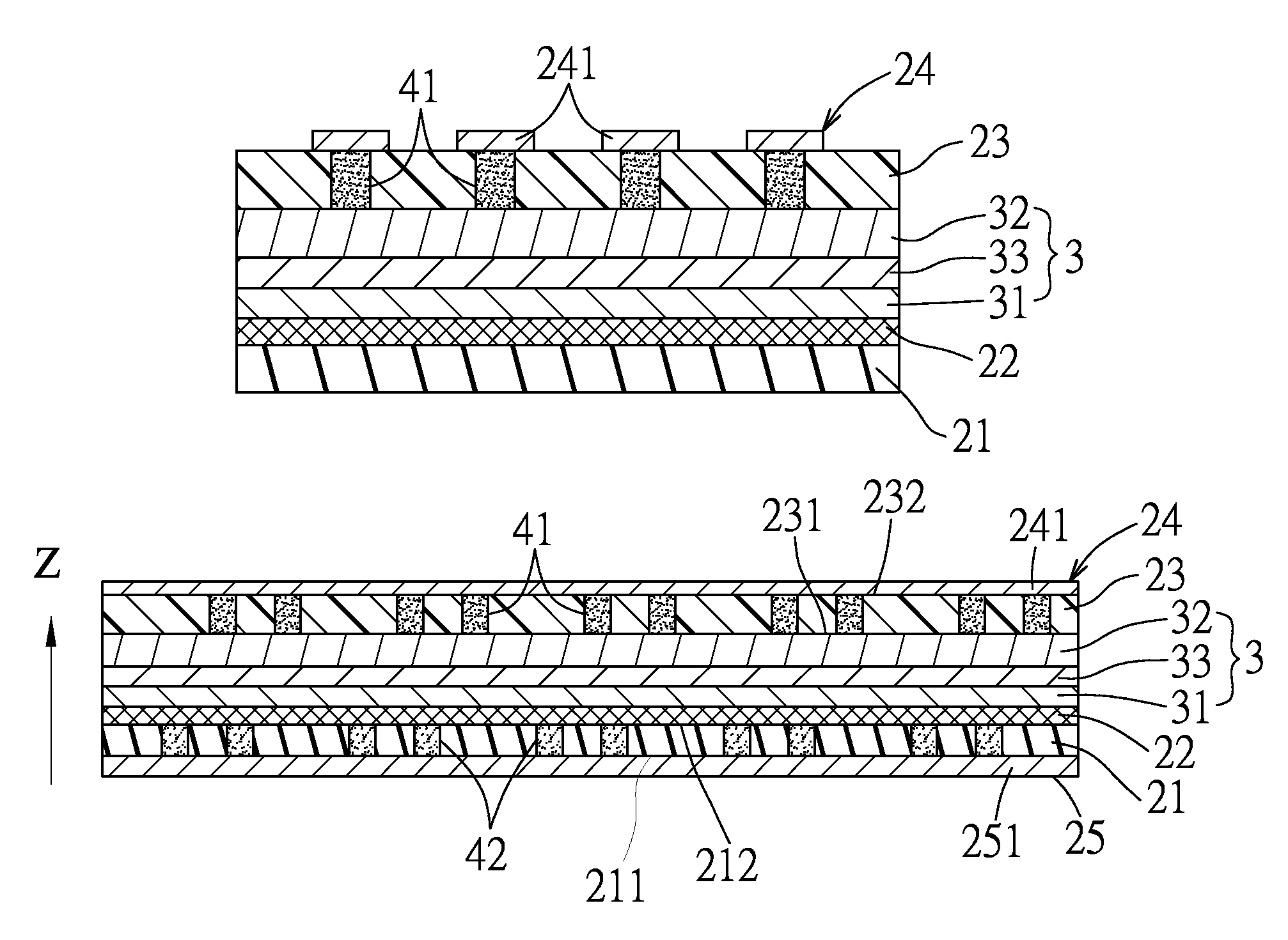
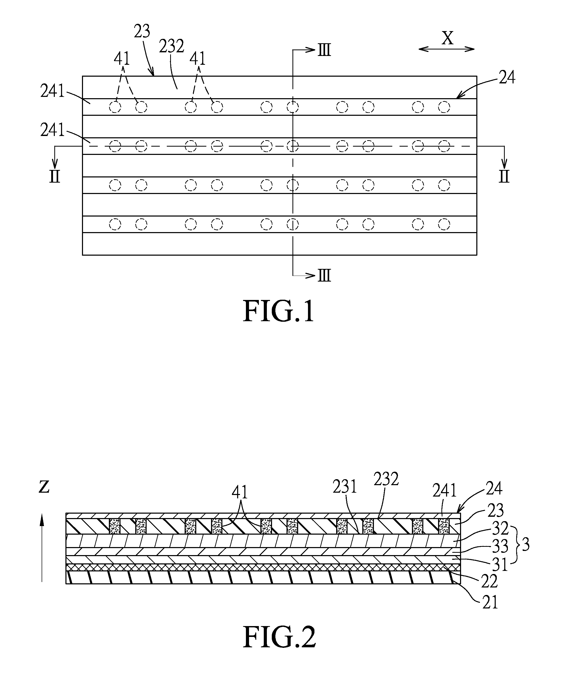
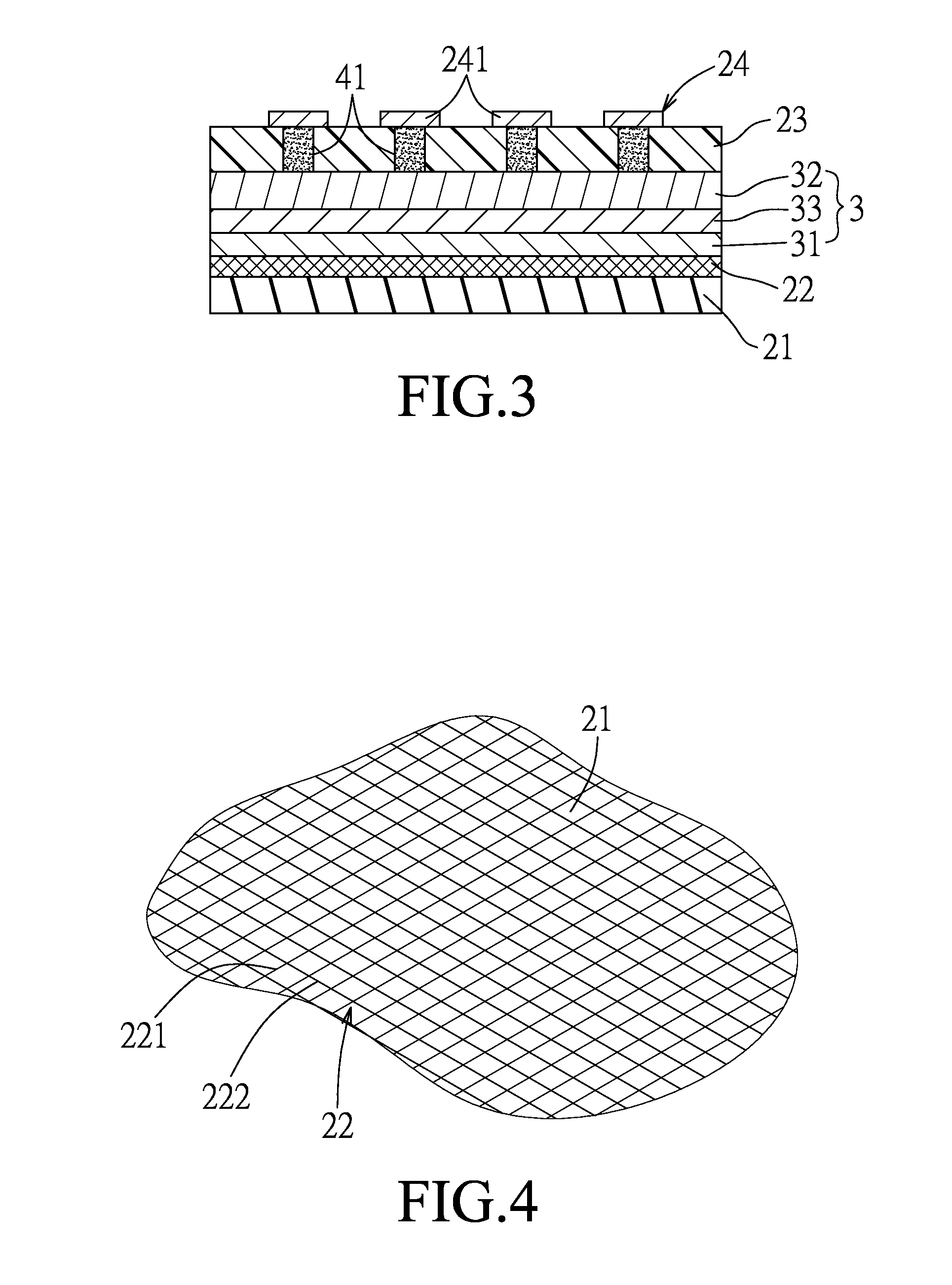
[0017]FIGS. 1 to 4 illustrate the first preferred embodiment of an OLED device according to this invention. The OLED device includes: a first insulator sheet 21; a light-emitting stack 3 stacked with the first insulator sheet 21 and including a transparent anode layer 31, a cathode layer 32, and a functional layer 33 stacked between the anode layer 31 and the cathode layer 32 in a vertical direction (Z) and made from an organic electroluminescent material; a metallic mesh 22 stacked with the anode layer 31 in the vertical direction (Z) and including a plurality of spaced apart first metallic nano-wires 221 and a plurality of spaced apart second metallic nano-wires 222 intersecting the first metallic nano-wires 221 (see FIG. 4), the metallic mesh 22 ...


PUM


Abstract

An OLED device includes: a first insulator sheet; a light-emitting stack stacked with the first insulator sheet and including a transparent anode layer, a cathode layer, and a functional layer; a metallic mesh stacked with the anode layer in a vertical direction, the metallic mesh contacting the anode layer and being covered by the anode layer; a second insulator sheet stacked with the cathode layer in the vertical direction; a plurality of cathode-connecting vias extending through the second insulator sheet; and a cathode-connecting metallic layer stacked with the second insulator sheet in the vertical direction and connected electrically to the cathode layer through the cathode-connecting vias.

Description

BACKGROUND OF THE INVENTION[0001]1. Field of the Invention[0002]This invention relates to an organic light emitting diode device, more particularly to an organic light emitting diode device including an anode layer and a metallic mesh stacked with the anode layer.[0003]2. Description of the Related Art[0004]Organic light emitting diodes (OLEDs) are useful for lighting. A conventional OLED device normally includes a transparent substrate, a transparent anode layer of indium tin oxide (ITO) formed on the transparent substrate, an active (or functional) layer of a conductive polymer formed on the anode layer, and a cathode layer formed on the active layer. The conventional OLED device is electrically activated by injecting an electric current to a peripheral side of the anode layer through a metallic busbar which is connected to an external power source. Since ITO has a much higher resistivity compared to a metallic material, the anode layer may suffer from a poor current distribution ...

Claims


Application Information

Patent Timeline
IPC IPC(8): H01L29/08H01L51/52
CPCH01L51/5209H01L51/5221Y02E10/549H10K59/40H10K77/111H10K50/814H10K50/824H10K50/805
Inventor CHANG, YIH
Owner AROLLTECH
Why Eureka
Try Eureka