Method for producing a thin-film semiconductor body and thin-film semiconductor body

Active Publication Date: 2015-12-01
OSRAM OPTO SEMICONDUCTORS GMBH & CO OHG
View PDF28 Cites 0 Cited by
  • Summary
  • Abstract
  • Description
  • Claims
  • Application Information

AI Technical Summary

Benefits of technology

[0016]Filling of the recesses and / or application of the semiconductor layer sequence likewise preferably proceeds by means of an epitaxial growth process. Particularly preferably, both steps, i.e., filling of the recesses and application of the semiconductor layer sequence, proceed by means of an epitaxial growth process. This embodiment of the method offers the advantage that production of the thin-film semiconductor body proceeds predominantly or completely by means of an epitaxy process. This advantageously simplifies production of the thin-film semiconductor body.
[0028]The outcoupling structures are provided to increase the outcoupling of electromagnetic radiation, generated in the active layer, from the thin-film semiconductor body.

Problems solved by technology

However, these semiconductor bodies are not thin-film semiconductor bodies.

Method used


Image

  • Method for producing a thin-film semiconductor body and thin-film semiconductor body
  • Method for producing a thin-film semiconductor body and thin-film semiconductor body
  • Method for producing a thin-film semiconductor body and thin-film semiconductor body

Examples


Embodiment Construction

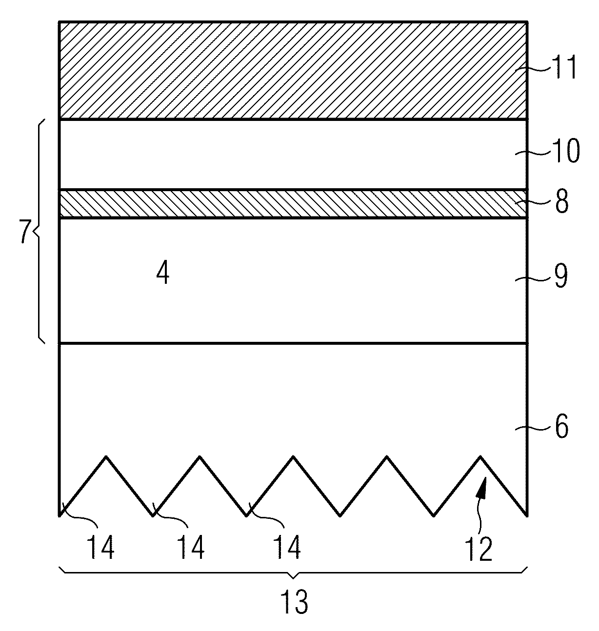
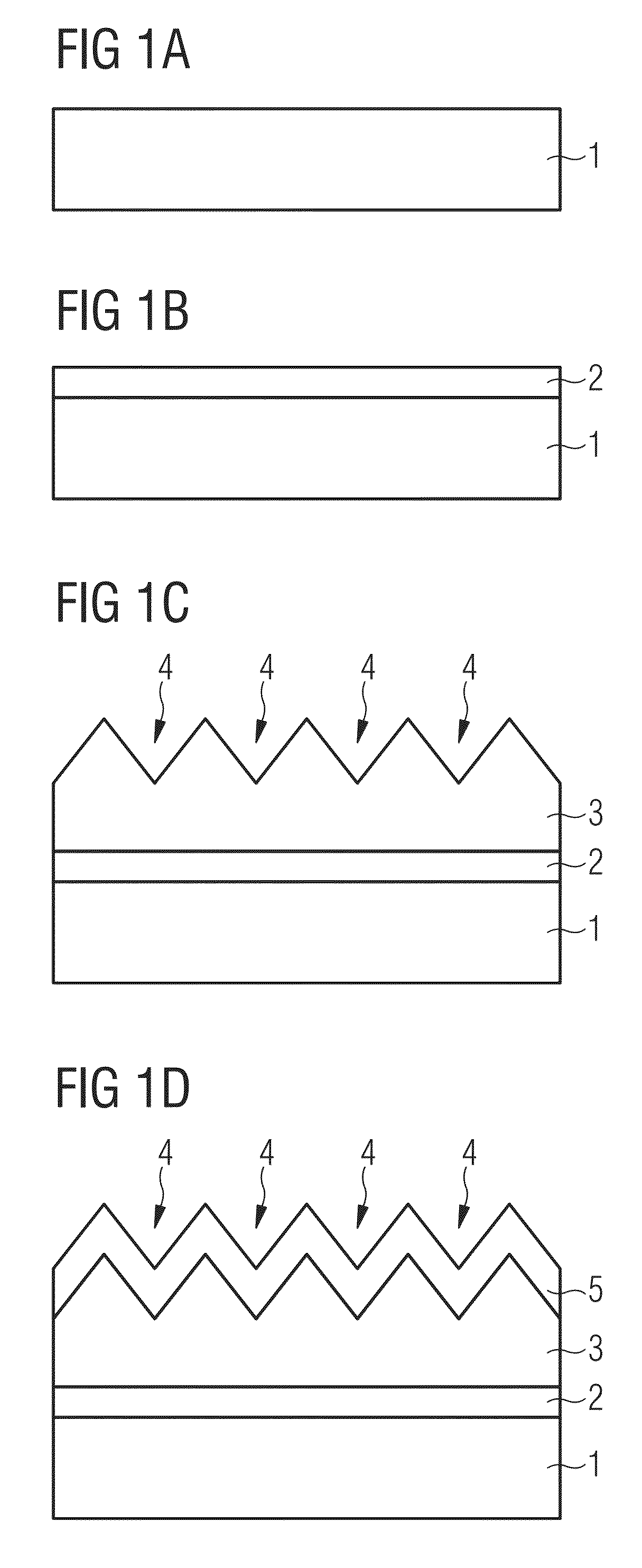
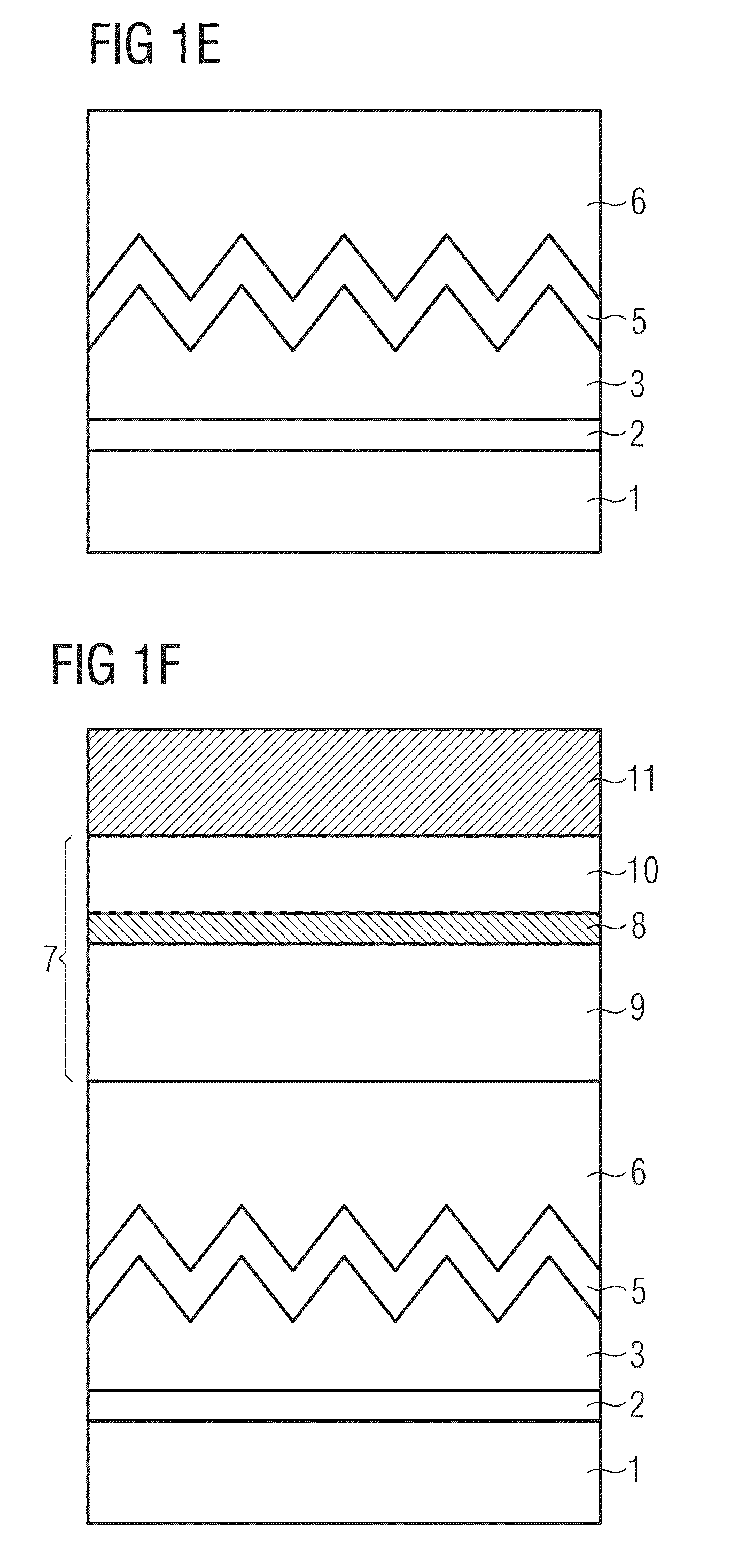
[0036]In the method according to the exemplary embodiment of FIGS. 1A to 1I, in a first step a growth substrate 1 is provided (FIG. 1A). The growth substrate 1 may, for example, contain sapphire, silicon, gallium nitride or silicon carbide or be formed of one of these materials.

[0037]In a next step a seed layer 2 is applied epitaxially onto the growth substrate 1 (FIG. 1B). The seed layer 2 is here formed of gallium nitride.

[0038]In a next step a buffer layer 3, which is here likewise formed of gallium nitride, is applied epitaxially onto the seed layer 2. On epitaxial application of the buffer layer 3, the growth conditions are adjusted such that recesses 4 form, which have the shape of inverted right pyramids with a regular hexagon as base (FIG. 1C). To this end, the temperature during epitaxial deposition here amounts to 850 C.

[0039]In a next method step, a continuous stop layer 5 is applied in direct contact onto the recesses 4 (FIG. 1D). In the process, the shape of the recesse...


PUM


Abstract

A method for producing a thin-film semiconductor body is provided. A growth substrate is provided. A semiconductor layer with funnel-shaped and / or inverted pyramid-shaped recesses is epitaxially grown onto the growth substrate. The recesses are filled with a semiconductor material in such a way that pyramid-shaped outcoupling structures arise. A semiconductor layer sequence with an active layer is applied on the outcoupled structures. The active layer is suitable for generating electromagnetic radiation. A carrier is applied onto the semiconductor layer sequence. At least the semiconductor layer with the funnel-shaped and / or inverted pyramid-shaped recesses is detached, such that the pyramid-shaped outcoupling structures are configured as projections on a radiation exit face of the thin-film semiconductor body.

Description

[0001]This patent application is a national phase filing under section 371 of PCT / EP2012 / 053348, filed Feb. 28, 2012, which claims the priority of German patent application 10 2011 012 928.6, filed Mar. 3, 2011, each of which is incorporated herein by reference in its entirety.TECHNICAL FIELD[0002]A method for producing a thin-film semiconductor body and a thin-film semiconductor body are provided.BACKGROUND[0003]Radiation-emitting semiconductor bodies are provided, for example, in German Patent Publication Nos. DE 10 2005 056 604 A1 and DE 10 2005 013 580 A1. However, these semiconductor bodies are not thin-film semiconductor bodies.SUMMARY OF THE INVENTION[0004]Embodiments of the present invention provide a method for producing a thin-film semiconductor body with well-defined outcoupling structures on the radiation exit face thereof. Furthermore, embodiments provide a corresponding thin-film semiconductor body.[0005]A method for producing a thin-film semiconductor body comprises a...

Claims


Application Information

Patent Timeline
Patent Type & Authority Patents(United States)
IPC IPC(8): H01L29/06H01L33/22H01L21/02H01L33/20H01L33/00
CPCH01L33/0075H01L21/0237H01L21/0254H01L21/02458H01L21/02494H01L21/02664H01L33/007H01L33/20H01L33/22H01L21/02502H01L2933/0091
Inventor LEIRER, CHRISTIANVOGL, ANTONBIEBERSDORF, ANDREASBUTENDEICH, RAINERRUMBOLZ, CHRISTIAN
Owner OSRAM OPTO SEMICONDUCTORS GMBH & CO OHG
Why Eureka
Try Eureka