

Method of inspecting a solder joint
a solder joint and inspection method technology, applied in the direction of instruments, manufacturing tools, image enhancement, etc., can solve the problem of lowering the reliability of inspection, and achieve the effect of improving inspection reliability
- Summary
- Abstract
- Description
- Claims
- Application Information
AI Technical Summary
Benefits of technology
Problems solved by technology
Method used
Image

Examples
Embodiment Construction
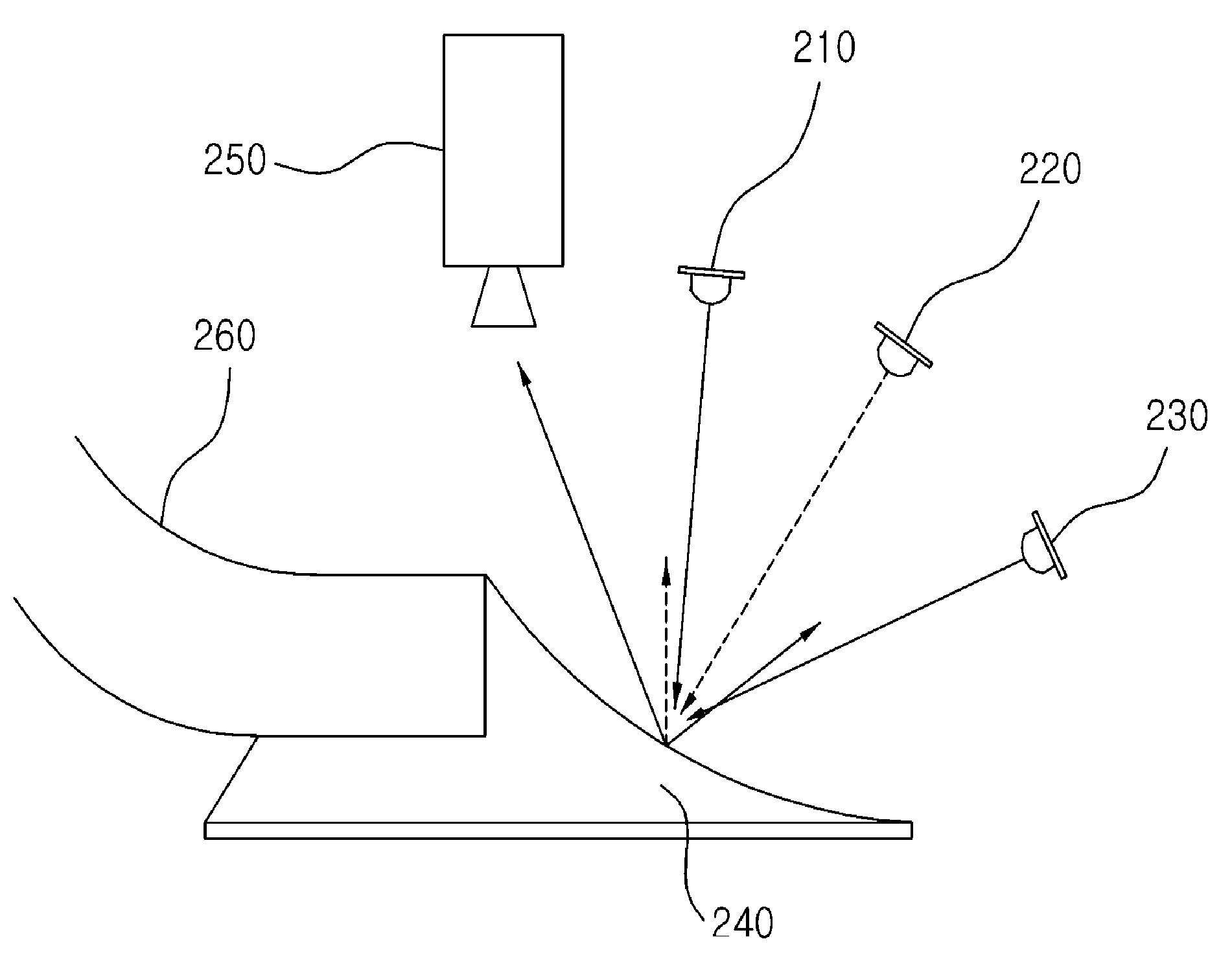
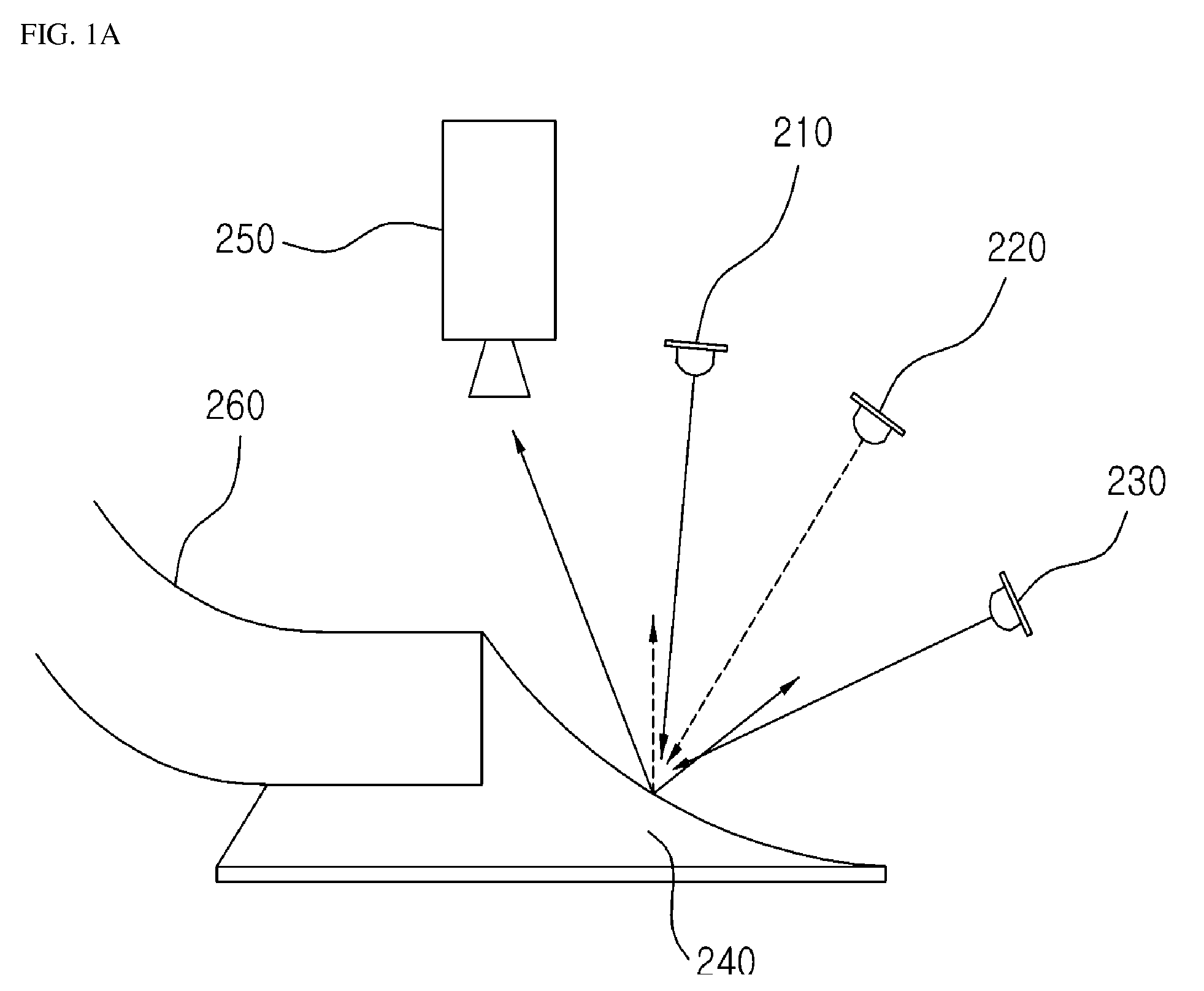
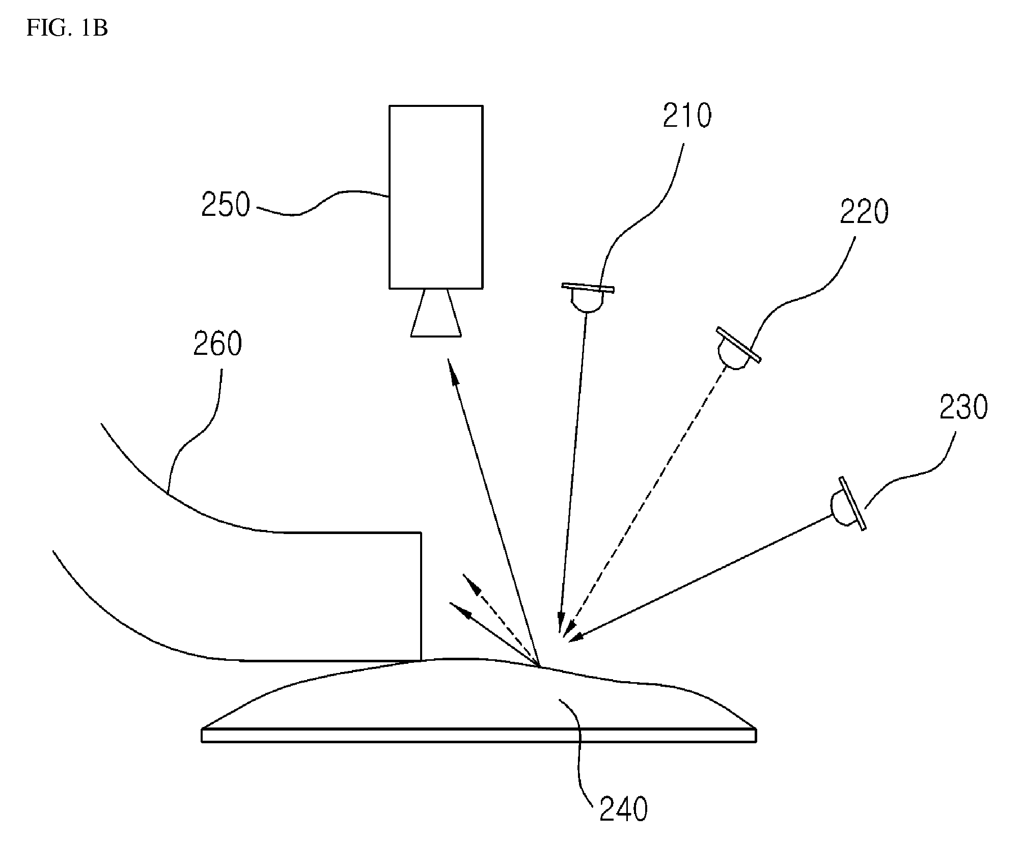
[0023]The present invention is described more fully hereinafter with reference to the accompanying drawings, in which example embodiments of the present invention are shown. The present invention may, however, be embodied in many different forms and should not be construed as limited to the example embodiments set forth herein. Rather, these example embodiments are provided so that this disclosure will be thorough and complete, and will fully convey the scope of the present invention to those skilled in the art. In the drawings, the sizes and relative sizes of layers and regions may be exaggerated for clarity.
[0024]It will be understood that, although the terms first, second, third etc. may be used herein to describe various elements, components, regions, layers and / or sections, these elements, components, regions, layers and / or sections should not be limited by these terms. These terms are only used to distinguish one element, component, region, layer or section from another region...
PUM
| Property | Measurement | Unit |
|---|---|---|
| thickness | aaaaa | aaaaa |
| height | aaaaa | aaaaa |
| color | aaaaa | aaaaa |
Abstract
Description
Claims
Application Information