Power conversion device control device

a technology of power conversion device and control device, which is applied in the direction of power conversion system, electronic switching, pulse technique, etc., can solve the problems of increased length of pulse width of error detection signal, increased manufacturing cost, and inability to carry out normal error detection

Active Publication Date: 2015-12-29
FUJI ELECTRIC CO LTD
View PDF22 Cites 5 Cited by
  • Summary
  • Abstract
  • Description
  • Claims
  • Application Information

AI Technical Summary

Benefits of technology

[0012]Therefore, aspects of the invention, having been contrived focusing on the unsolved problems of the heretofore known examples, can provide a power conversion device control device with which it is possible to accurately determine the protection operation condition of plural protection circuits, with a simple configuration and with no erroneous detection.
[0031]According to aspects of the invention, when plural protection circuits that detect information necessary in order to carry out a protection operation of a semiconductor element are provided in a power conversion device control device that individually drives semiconductor elements configuring a power conversion device, a protection circuit for which it is first detected that a protection operation is necessary is taken as a first-come first-served protection circuit, and a pulse signal with a cycle in which are combined a determination period corresponding to the protection circuit and a constant period is output as an alarm signal. A condition that a protection operation stopped condition, wherein it is detected that no protection operation is necessary in at least the first-come first-served protection circuit, is met is taken as a resetting condition of the alarm signal, and a determination of the resetting condition is carried out during the constant period of the pulse signal. Because of this, an advantage is obtained in that it is possible to reliably prevent the alarm signal from being affected by a protection circuit for which it is subsequently detected that a protection operation is necessary, and it is possible to reliably prevent the alarm signal from finishing partway through a determination period of the pulse signal configuring the alarm signal, thus enabling the formation of an accurate alarm signal.

Problems solved by technology

However, in the heretofore known example described in PTL 1, an overheat failure, overcurrent failure, short circuit failure, and insufficient voltage failure of the power transistor module are detected individually, pulse signals of differing pulse widths are supplied to an OR gate, and a collective failure detection signal is output from the OR gate.
Because of this, even though an overheat failure, overcurrent failure, short circuit failure, and insufficient voltage failure are detected individually, and pulse signals of differing pulse widths are output, each pulse signal is passed through the OR gate and formed into a collective failure detection signal, meaning that when another error occurs in a condition in which plural errors are occurring simultaneously, or one error is occurring, there is an unsolved problem in that the pulse width of the error detection signal increases in length, and it is not possible to carry out a normal error detection.
Because of this, it is possible to solve the unsolved problem of PTL 1, but there is an unsolved problem in that it is necessary to form plural output terminals, and the manufacturing cost soars.
However, with PTL 3, when configuring, for example, a three-phase inverter with six identical driver ICs, there is an unsolved problem in that a transmission circuit that collects and processes signals from each driver IC is needed, and the manufacturing cost soars.

Method used


Image

  • Power conversion device control device
  • Power conversion device control device
  • Power conversion device control device

Examples


first embodiment

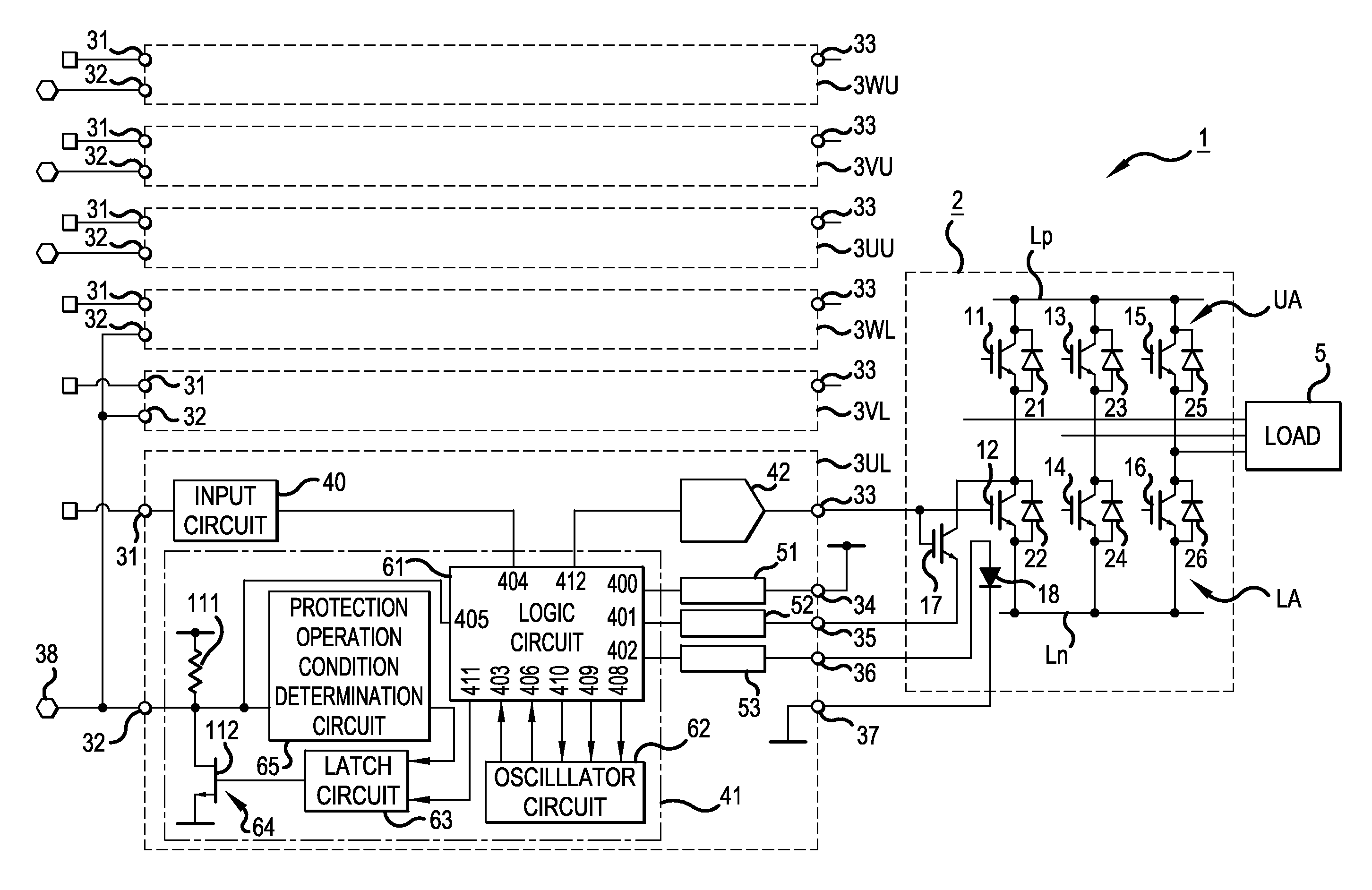
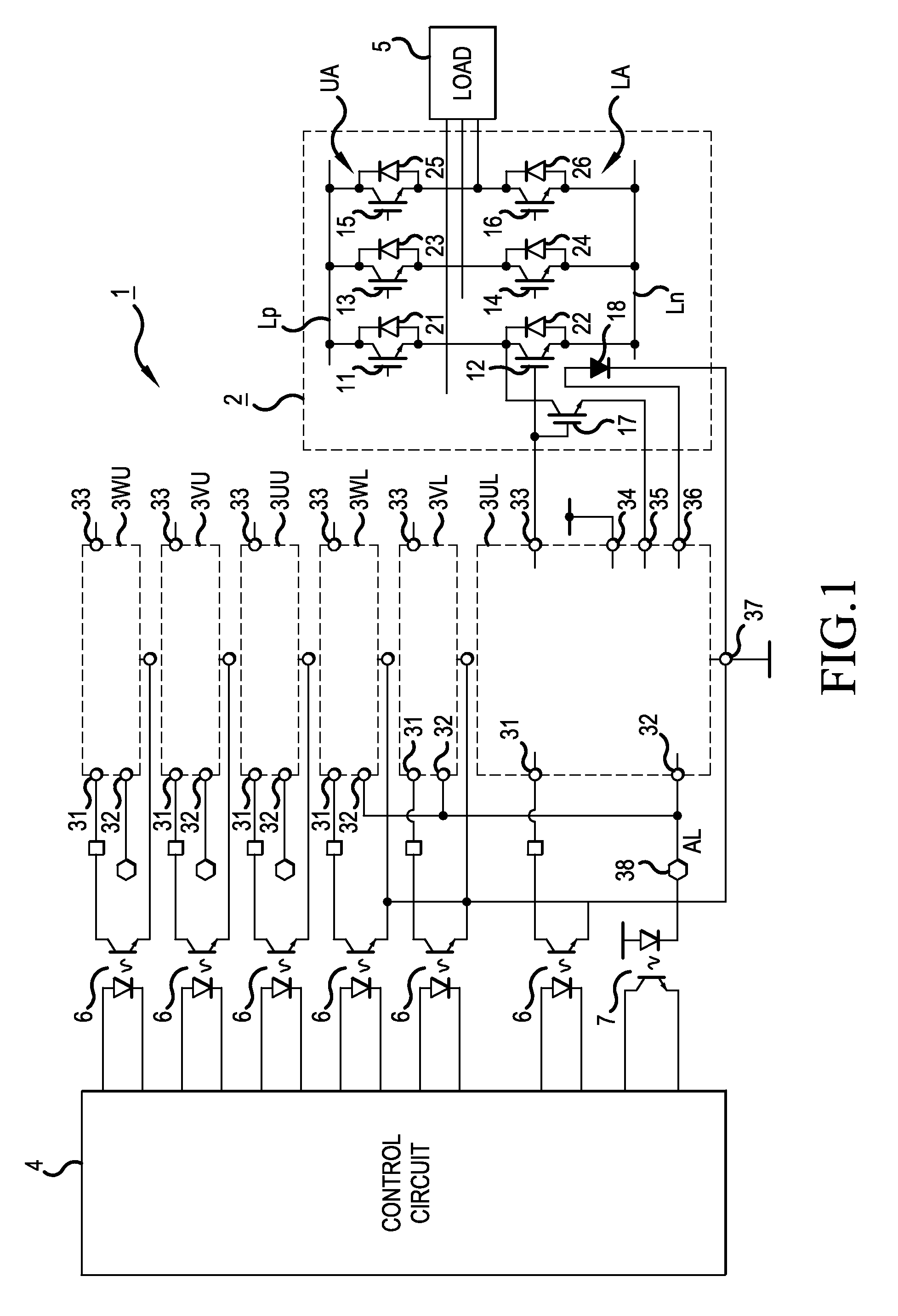
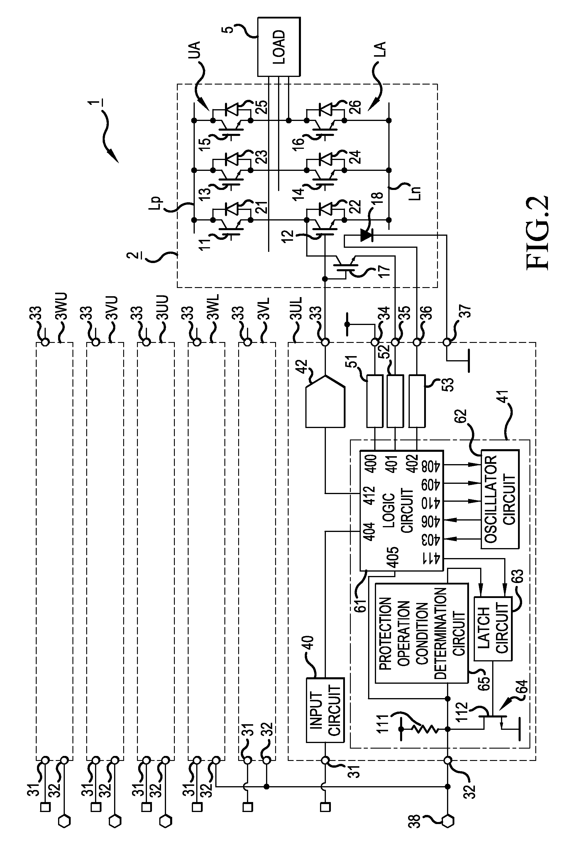
[0093]Next, a description will be given of an operation of the

[0094]Now, it is assumed that the current flowing through the IGBTs 11 to 16 configuring the inverter 2 is below the overcurrent threshold value and normal, that the temperature in the chip in which the IGBTs 11 to 16 are formed is below the overheat threshold value and normal, and furthermore, that the IC power supply voltage supplied to the driver ICs 3UL to 3WL and 3UU to 3WU exceeds the low voltage threshold value and is normal.

[0095]In this normal condition, the protection operation signals H1, H2, and H3 output from the low voltage protection circuit 51, overcurrent protection circuit 52, and overheat protection circuit 53 of the driver ICs 3UL to 3WL and 3UU to 3WU are at a low level. At this time, when all of the RS type flip-flop circuits 416, 426, and 436 and 418, 428, and 438 are in a reset condition in the logic circuit 61, the output of the NOR gate 441 is at a high level. The high level output of the NOR gat...

second embodiment

[0151]Next, a description will be given, referring to FIGS. 10 and 11, of the invention.

[0152]In the second embodiment, instead of the case of setting the determination periods of the pulse signals PS1 to PS3 to differing values, the numbers of pulses are set to differing values.

[0153]That is, in the second embodiment, the oscillator circuit 62 is configured as shown in FIG. 10.

[0154]In the oscillator circuit 62, the determination period signal formation circuits 520 and 540 of the first embodiment are omitted, and the configuration of the determination period signal formation circuit 500 is changed instead.

[0155]That is, as shown in FIG. 10, the determination period signal formation circuit 500 is such that a combination of a series circuit of PMOS-FETs 591 and 592 and a series circuit of PMOS-FETs 593 and 594 is connected in parallel to the PMOS-FETs 505 and 507 configuring a current mirror circuit.

[0156]Also, the gates of the PMOS-FETs 591 and 593 are connected to the gates of th...


PUM


Abstract

Aspects of the invention include a power conversion device control device, including multiple drive circuits having an alarm signal formation circuit that sets a pulse signal having as one cycle a period. The one cycle period includes a determination period, of which a different period is set for each of plural protection circuits that detect information for carrying out a protection operation of semiconductor elements configuring a power conversion device, and a constant period, in which a condition varies with respect to the determination period, takes a protection circuit for which it is first detected that a protection operation is necessary to be a first-come first-served protection circuit, and outputs the pulse signal corresponding to the first-come first-served protection circuit as an alarm signal, wherein the alarm signal formation circuit is such that a resetting condition of the alarm signal is a condition that a protection operation stopped condition.

Description

CROSS-REFERENCE TO RELATED APPLICATIONS[0001]This application is a continuation of International Application No. PCT / JP2012 / 002427, filed on Apr. 6, 2012, which is based on and claims priority to Japanese Patent Application No. JP PA 2011-086717, filed on Apr. 8, 2011. The disclosure of the Japanese priority application and the PCT application in their entirety, including the drawings, claims, and the specification thereof, are incorporated herein by reference.BACKGROUND[0002]1. Field of the Invention[0003]Aspects of the invention relate to power conversion device control devices that drive semiconductor elements.[0004]2. Related Art[0005]As this kind of power conversion device control device, there is known, for example, a power transistor module failure determination method of individually determining failure causes by giving pulse widths of failure detection signals differing setting times in accordance with an overheat failure, an overcurrent failure, a short circuit failure, an...

Claims


Application Information

Patent Timeline
Patent Type & Authority Patents(United States)
IPC IPC(8): H02H7/00H02H9/00H03K17/082H03K17/18H02M1/084H02M1/32H02H9/02H02H3/20
CPCH02M1/32H03K17/18H03K17/0828H02M1/084H02M7/48
Inventor NAKAMORI, AKIRA
Owner FUJI ELECTRIC CO LTD
Why Eureka
Try Eureka