
IGZO devices with composite channel layers and methods for forming the same

a technology of indiumgalliumzinc oxide and composite channel layer, which is applied in the direction of semiconductor devices, electrical devices, transistors, etc., can solve the problems of affecting the performance of the device and relatively high contact resistivity

Inactive Publication Date: 2016-01-26
INTERMOLECULAR
View PDF8 Cites 15 Cited by
  • Summary
  • Abstract
  • Description
  • Claims
  • Application Information

AI Technical Summary

Benefits of technology

The present invention relates to methods for forming indium-gallium-zinc oxide (IGZO) devices, such as thin-film transistors (TFTs), with improved electrode contact resistivity while still maintaining high channel mobility. The invention proposes methods for forming composite channel layers or bi-layers of a-IGZO and crystalline IGZO to reduce contact resistivity with the source and drain electrodes. The techniques described herein can help to address the challenge of high contact resistivity with the source and drain electrodes that may inhibit the performance of the device. The invention is useful for applications such as display devices, where the use of crystalline IGZO is favored over other materials due to its stability and compatibility with transparent, flexible, and light display applications.

Problems solved by technology

However, the use of crystalline IGZO may inhibit the performance of the device to relatively high contact resistivity with the source and drain electrodes.

Method used


Image

  • IGZO devices with composite channel layers and methods for forming the same
  • IGZO devices with composite channel layers and methods for forming the same
  • IGZO devices with composite channel layers and methods for forming the same

Examples


Embodiment Construction

[0015]A detailed description of one or more embodiments is provided below along with accompanying figures. The detailed description is provided in connection with such embodiments, but is not limited to any particular example. The scope is limited only by the claims and numerous alternatives, modifications, and equivalents are encompassed. Numerous specific details are set forth in the following description in order to provide a thorough understanding. These details are provided for the purpose of example and the described techniques may be practiced according to the claims without some or all of these specific details. For the purpose of clarity, technical material that is known in the technical fields related to the embodiments has not been described in detail to avoid unnecessarily obscuring the description.

[0016]The term “horizontal” as used herein will be understood to be defined as a plane parallel to the plane or surface of the substrate, regardless of the orientation of the ...


PUM


Abstract

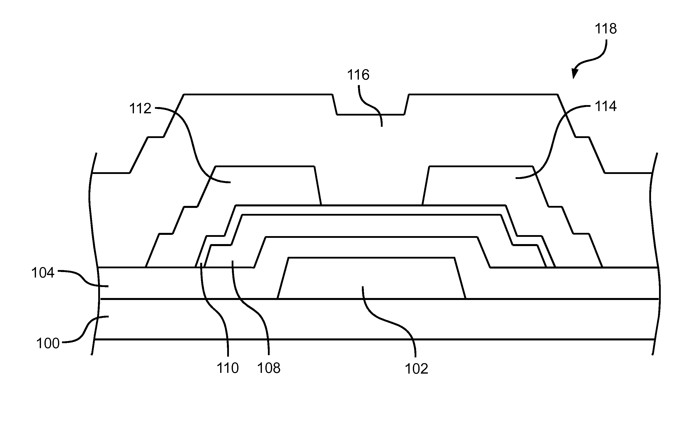
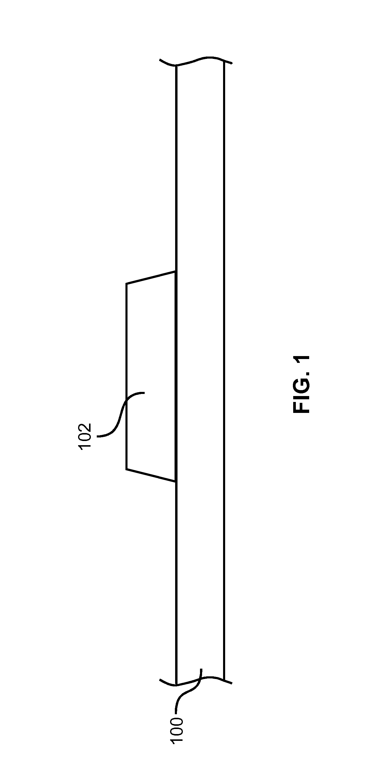
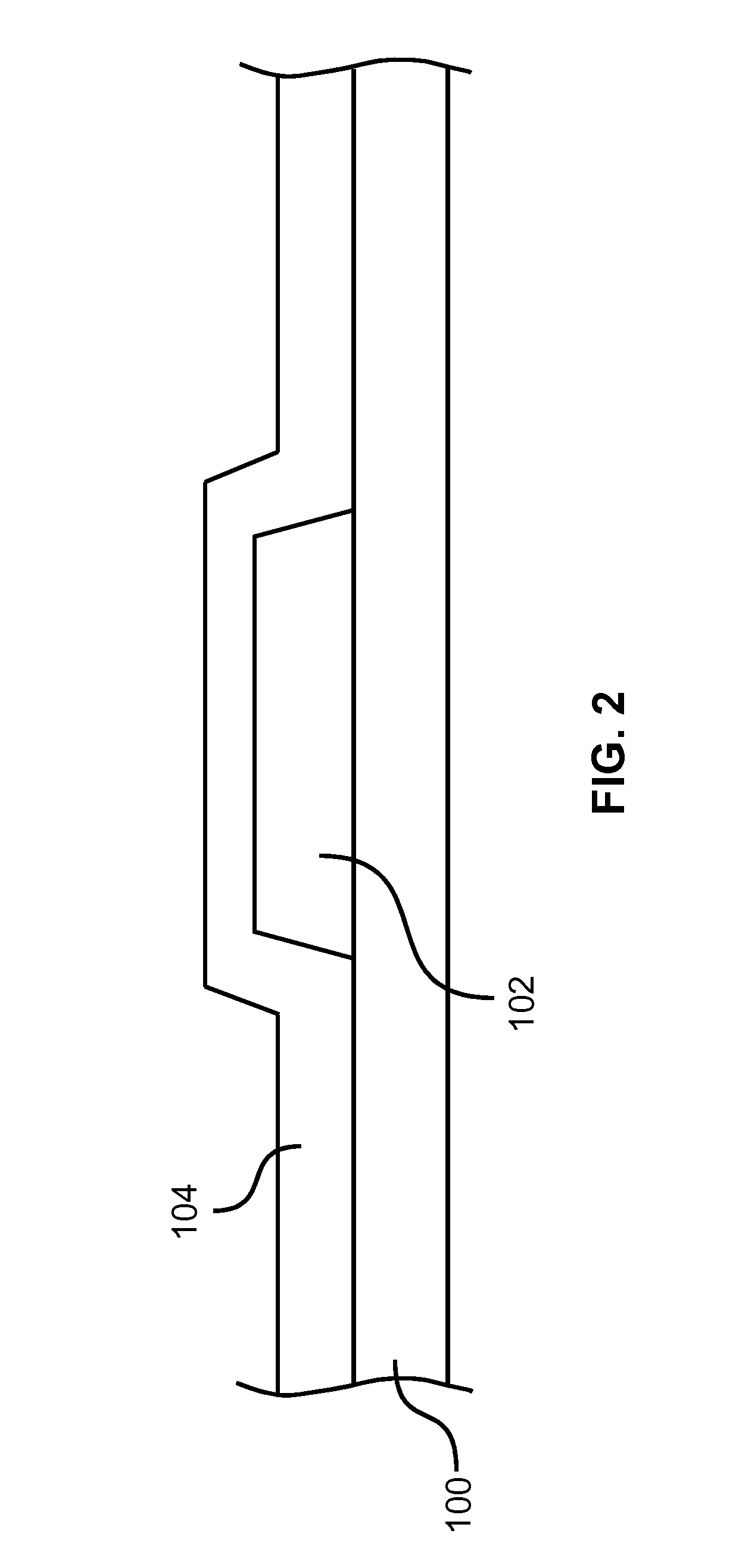
Embodiments described herein provide indium-gallium-zinc oxide (IGZO) devices, such as IGZO thin-film transistors (TFTs), and methods for forming such devices. A substrate is provided. A gate electrode is formed above the substrate. An IGZO channel layer is formed above the gate electrode. The IGZO channel layer has a first sub-layer including c-IGZO and a second sub-layer including a-IGZO. A source electrode and a drain electrode are formed above the IGZO channel layer.

Description

TECHNICAL FIELD[0001]The present invention relates to indium-gallium-zinc oxide (IGZO) devices. More particularly, this invention relates to methods for forming IGZO devices, such as thin-film transistors (TFTs), with composite channel layers and methods for forming such devices.BACKGROUND OF THE INVENTION[0002]Indium-gallium-zinc oxide (IGZO) devices, such as IGZO thin-film transistors (TFTs) have attracted a considerable amount of attention due to the associated low cost, room temperature manufacturing processes with good uniformity control, high mobility for high speed operation, and the compatibility with transparent, flexible, and light display applications. Due to these attributes, IGZO TFTs may even be favored over low cost amorphous silicon TFTs and relatively high mobility polycrystalline silicon TFT for display device applications. IGZO devices typically utilize amorphous IGZO (a-IGZO).[0003]Recent developments in the field suggest that the use of crystalline IGZO may prov...

Claims


Application Information

Patent Timeline
Patent Type & Authority Patents(United States)
IPC IPC(8): H01L29/12H01L21/02H01L29/66H01L29/786
CPCH01L29/78693H01L21/02472H01L21/02483H01L21/02538H01L21/02554H01L21/02565H01L21/02592H01L21/02595H01L21/02631H01L29/66765H01L29/66969H01L29/7869H01L29/78696
Inventor AHMED, KHALED
Owner INTERMOLECULAR
Learn More