High density connector

a high-density, connector technology, applied in the direction of line/current collector details, coupling device connections, electrical apparatus, etc., can solve the problem of becoming more difficult to improve data rates, and achieve the effect of high performan

Active Publication Date: 2016-01-26
MOLEX INC
View PDF8 Cites 61 Cited by
  • Summary
  • Abstract
  • Description
  • Claims
  • Application Information

AI Technical Summary

Benefits of technology

[0004]A connector is disclosed that allows for very compact routing on a minimal number of layers while providing for high performance. In an embodiment, the connector includes pair of signal wafers that are positioned side-by side, each wafer including a first terminal with a contact, a tail and a body extending between the tail and contact so that a pair of the first terminals can form a differential pair. The differential pair can be configured to provide a broad-side coupled configuration in the body of the terminals. The tails are configured to be positioned in a line and the line can be positioned between the body of the different pairs. At least one of the wafers that forms the pair of wafers includes a tail stub that is electrically isolated from the first terminal and includes a tail. A ground wafer is provided adjacent one of the pair of wafers and can include one or more terminals that are arranged such that the body is aligned with the body of the terminals that provide the differential pair. The ground terminal omits a tail and instead the ground terminal is coupled to the tail stub in one of the signal wafers. A conductive member can connect a junction in the ground terminal to a junction in the tail stub.

Problems solved by technology

One major complication with this effort is that more closely arranged communication channels create cross-talk on neighboring channels, thus it becomes more challenging to improve data rates while providing for an increase in density that can actually be mounted on a circuit board.
In particular, ground vias (which are required to electrically connect to ground terminals) tend to be positioned in locations that interfere with ideal signal trace routing configurations.

Method used


Image

  • High density connector
  • High density connector
  • High density connector

Examples


Embodiment Construction

[0029]The detailed description that follows describes exemplary embodiments and is not intended to be limited to the expressly disclosed combination(s). Therefore, unless otherwise noted, features disclosed herein may be combined together to form additional combinations that were not otherwise shown for purposes of brevity.

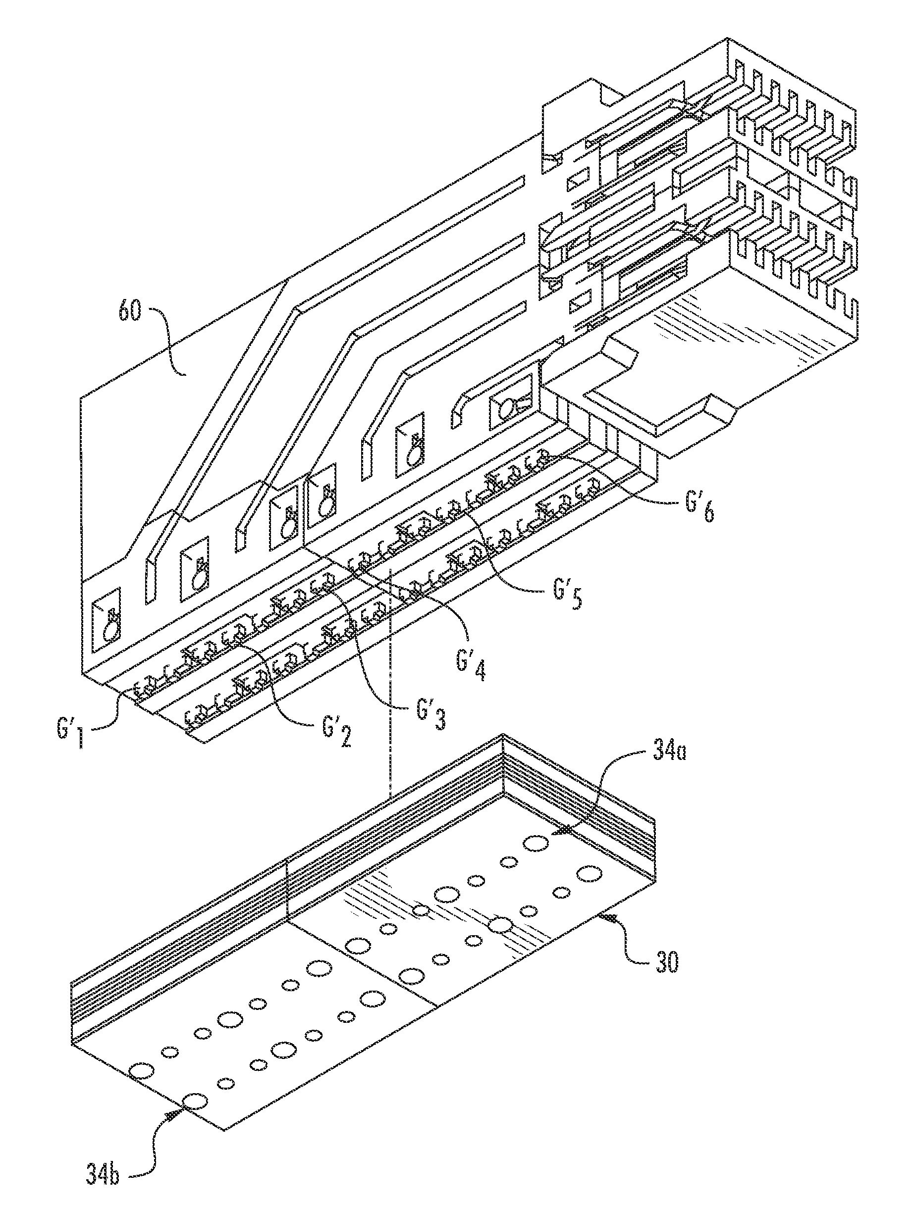
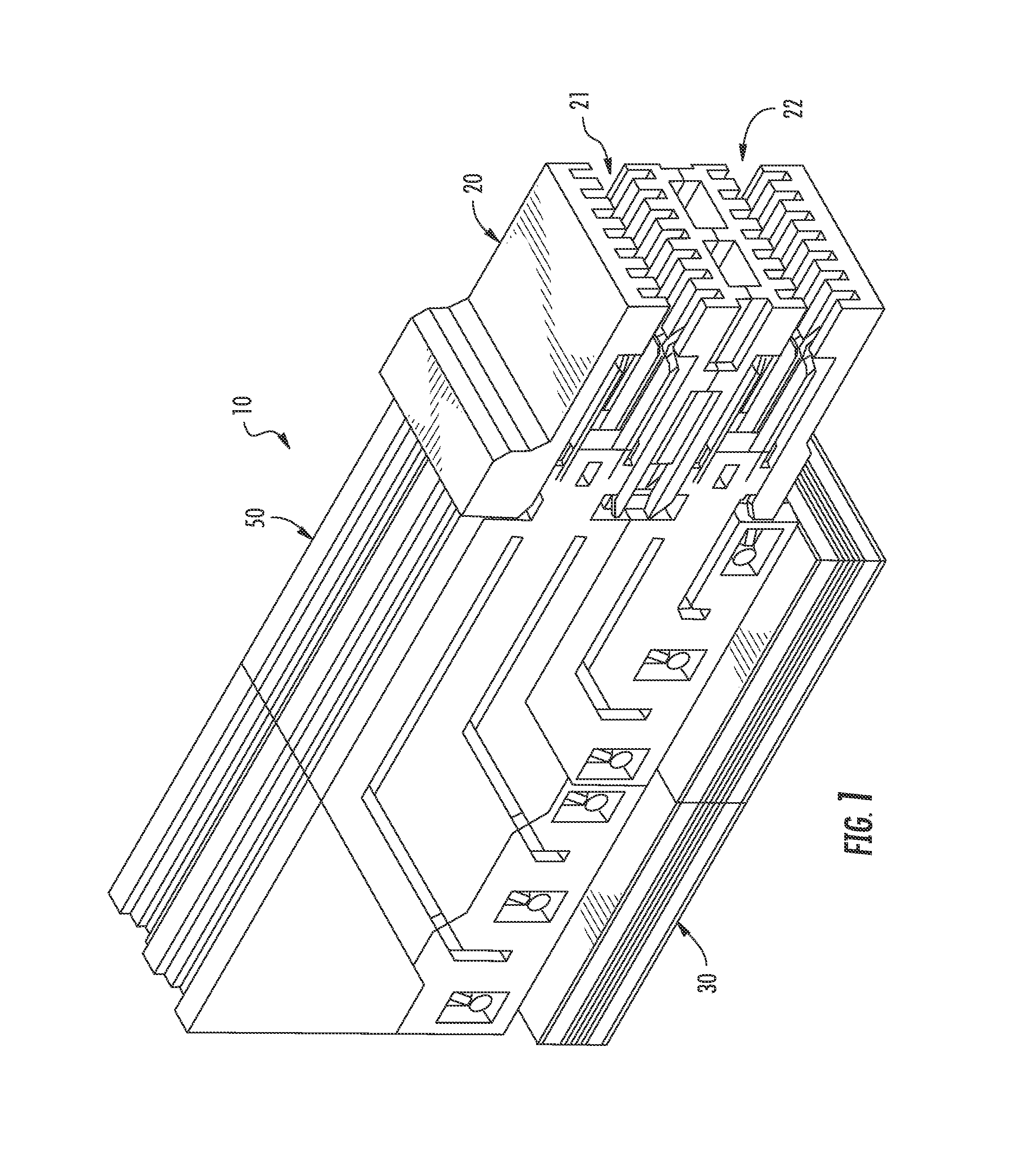
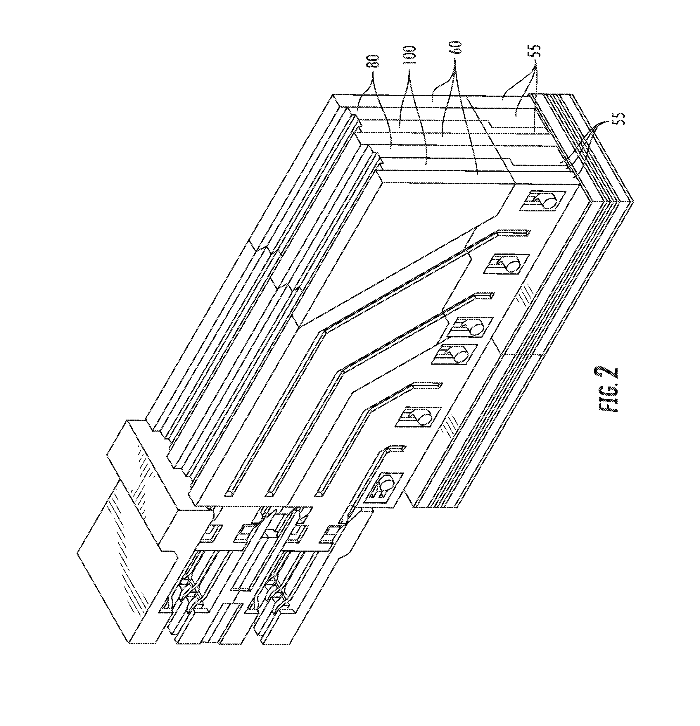
[0030]FIGS. 1-10B illustrate features of a first embodiment. As can be appreciated, a connector system 10 includes a set of wafers 50 supported by a housing 20 that is positioned on a circuit board 30. While a partial housing 20 is disclosed, the housing can include sides, a top and rear wall in addition to front portion that supports card slots. Thus, any desirable housing may be provided. It should be further appreciated that while a stacked connector (e.g., two or more vertically arranged card slots) is depicted with a first card slot 21 and a second card slot 22, a single card slot could also be provided. The card slot 21 can have a first side 21a and a second...


PUM


Abstract

A connector can be provided that allows for improved route-out including straight-back routing. Signal and ground terminal tails can be arranged in a single row to help facilitate such functionality. Consequentially, a connector with two vertically stacked card slots can be provided that allows for straight back routing of the signal traces in four layers while still providing a compact connector design.

Description

RELATED APPLICATIONS[0001]This application is a national phase of PCT Application No. PCT / US2013 / 039459, filed May 3, 2013, which in turn claims priority to U.S. Provisional Application No. 61 / 642,005, filed May 3, 2012, which is incorporated herein by reference in its entirety.FIELD OF THE INVENTION[0002]The present invention relates to the field of connectors, more specifically to the field of connectors suitable for use in applications where the connector is supported by a circuit board.DESCRIPTION OF RELATED ART[0003]Connectors are widely used to provide an interface between a circuit board and another connector (such as a plug connector). Due to the continual improvement in computing power and the increased demand for high bandwidth communication channels on the end user side, there has been increased demand for connectors that can handle higher density of transmission channels while at the same time there has been an increased desire to provide connectors that take up less spa...

Claims


Application Information

Patent Timeline
Patent Type & Authority Patents(United States)
IPC IPC(8): H01R13/514H01R12/71H01R9/24H01R12/72H01R12/70H01R13/652H01R13/6466H01R13/6471H01R13/658
CPCH01R12/71H01R9/2408H01R9/2458H01R12/7082H01R12/724H01R13/652H01R12/7076H01R43/205H01R13/6587
Inventor REGNIER, KENT E.CASHER, PATRICK R.ROWLANDS, MICHAEL
Owner MOLEX INC
Why Eureka
Try Eureka