Semiconductor device

a semiconductor device and semiconductor technology, applied in the direction of semiconductor devices, basic electric elements, electrical equipment, etc., can solve the problems of easy application of high thermal stress to the outer peripheral trench, and achieve the effects of promoting the extension of a depletion layer, and reducing the voltage of the semiconductor devi

Active Publication Date: 2016-03-08
DENSO CORP
View PDF11 Cites 1 Cited by
  • Summary
  • Abstract
  • Description
  • Claims
  • Application Information

AI Technical Summary

Benefits of technology

[0006]In this semiconductor device, the plurality of loop trenches is formed in the peripheral region, and the p-type fourth region is formed in the range in contact with the bottom surface of each of the loop trenches. Each of the fourth regions promotes extension of a depletion layer from a MOS structure toward the peripheral region when the MOS structure, having the first region, the second region, the third region, and the gate trench, is off. As a result, a withstand voltage of the semiconductor device is improved. Moreover, each of the loop trenches extends so as to surround the region smaller than the gate trench region in which the plurality of gate trenches is formed. Moreover, each of the loop trenches is separated from the other loop trenches. Since each of the loop trenches is finely separated as above, even if a temperature of the semiconductor device rises, thermal stress generated in each of the loop trenches is suppressed.

Problems solved by technology

Thus, high thermal stress can easily apply to the outer peripheral trench, which is a problem.

Method used


Image

  • Semiconductor device
  • Semiconductor device
  • Semiconductor device

Examples


embodiment 1

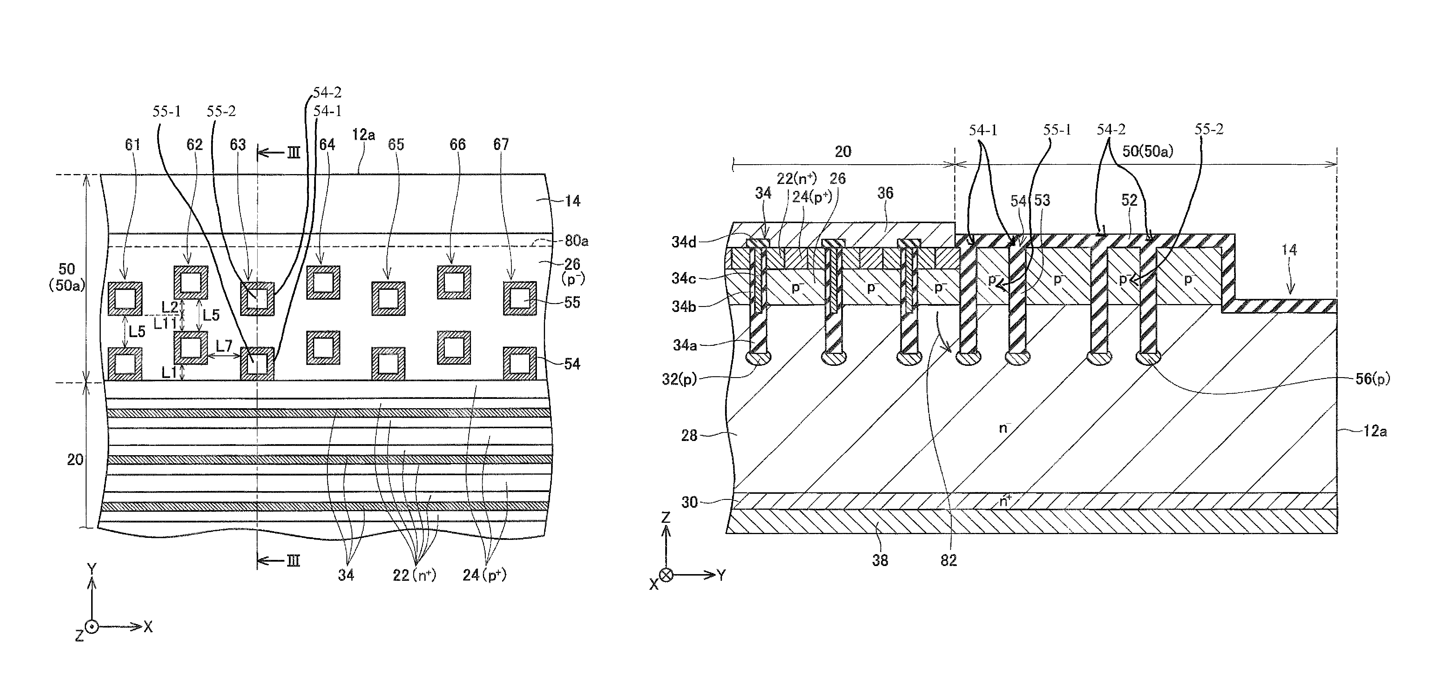
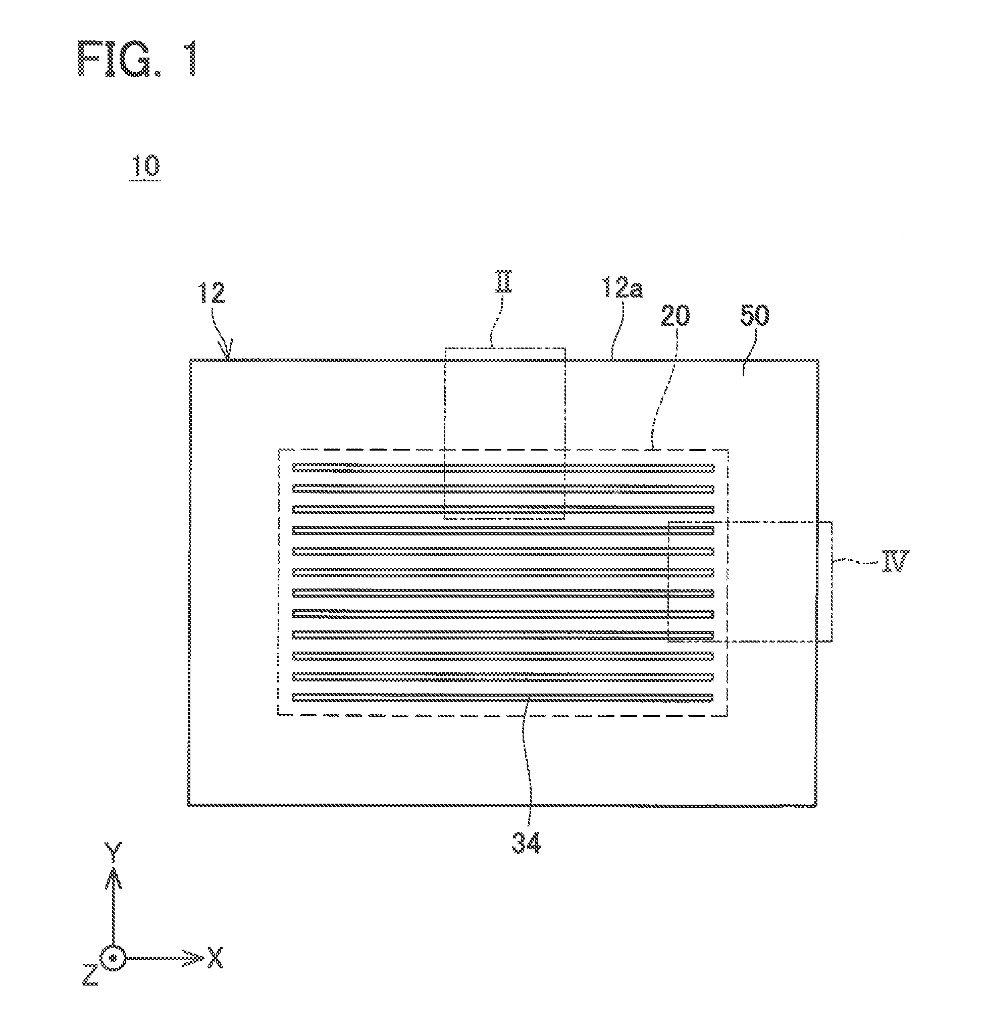
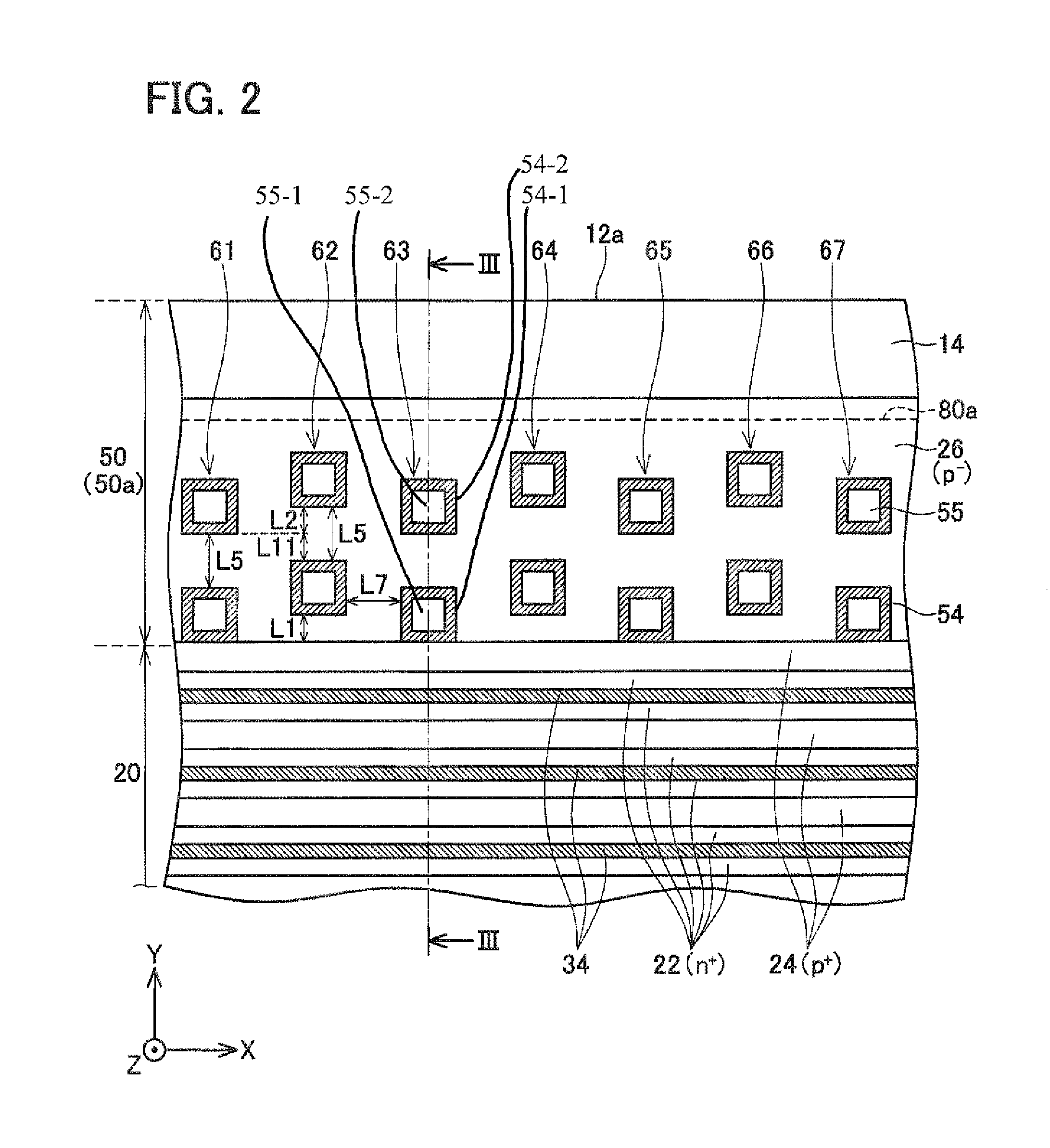
[0032]As illustrated in FIG. 1, a semiconductor device 10 according to Embodiment 1 has a semiconductor substrate 12 made of SiC. The semiconductor substrate 12 has a MOSFET region 20 and a peripheral region 50. A MOSFET is formed in the MOSFET region 20. It should be noted that only a gate trench 34 is illustrated in the MOSFET region 20 in FIG. 1 for ease of understanding of the drawing. Moreover, illustration of details in the peripheral region 50 is omitted in FIG. 1. The peripheral region 50 is a region between the MOSFET region 20 and an end surface 12a of the semiconductor substrate 12. It should be noted that, in each of the figures which will be explained below, an X-direction indicates a direction in which each of the gate trenches 34 extends (a longitudinal direction of the gate trenches 34) when an upper surface of the semiconductor substrate 12 is viewed on a plane, a Y-direction indicates a width direction of each of the gate trenches 34 (that is, a direction orthogona...

embodiment 2

[0056]In a semiconductor device in Embodiment 2, as illustrated in FIG. 9, one or more loop trenches 54a in the first peripheral region 50a have protruding portions 57a protruding outward from rectangles along sides extending in the X-direction, respectively. The protruding portion 57a extends toward the adjacent loop trench 54. Thus, an interval L9 between the adjacent loop trench 54 and the protruding portion 57a is narrowed. It should be noted that, since the p-type floating region 56 is formed along the loop trench 54, the p-type floating region 56 is formed also under the trench constituting the protruding portion 57a.

[0057]According to such configuration, extension of the depletion layer in the X-direction from the loop trench 54a is promoted by the p-type floating region 56 located under the protruding portion 57a. As a result, the depletion layer can be made to reliably extend to a portion indicated by the interval L9. Moreover, though the interval L9 is narrowed by the pro...

embodiment 3

[0059]In a semiconductor device in Embodiment 3, as illustrated in FIG. 11, the protruding portion 57a of the loop trench 54a extends toward a region between two loop trenches 54c and 54d of the adjacent groups in the first peripheral region 50a. That is, an extended line of the protruding portion 57a does not intersect the adjacent loop trenches 54c. Since a region surrounded by the loop trenches 54a, 54c, and 54d is far from any of the loop trenches 54, this is a region in which the depletion layer cannot extend easily. Since the protruding portion 57a extends toward such region, according to the configuration of Embodiment 3, the depletion layer can be made to extend into the first peripheral region 50a more reliably.

[0060]Moreover, in the semiconductor device in Embodiment 3, as illustrated in FIG. 12, the protruding portion 57b of the loop trench 54b extends toward a region between two loop trenches 54e and 54f of the adjacent groups in the second peripheral region 50b. As desc...


PUM


Abstract

A trench structure which is capable of promoting extension of a depletion layer and hardly causes thermal stress is provided. A semiconductor device includes a semiconductor substrate. A plurality of loop trenches is formed on the surface of the semiconductor substrate. Each loop trench is configured to extend so as to surround a region smaller than the region where a plurality of gate trenches is formed. Each loop trench is separated from other loop trenches. A second insulating layer is located in each loop trench. P-type fourth regions are formed in the semiconductor substrate. Each fourth region is in contact with a bottom surface of corresponding one of the loop trenches and is configured to extend along the corresponding one of the loop trenches.

Description

CROSS-REFERENCE TO RELATED APPLICATION[0001]This application claims priority to Japanese Patent Application No. 2013-234341 filed on Nov. 12, 2013, the contents of which are hereby incorporated by reference into the present application.TECHNICAL FIELD[0002]A technology disclosed in this description relates to a semiconductor device.DESCRIPTION OF RELATED ART[0003]The semiconductor device disclosed in Japanese Patent Application Publication No. 2005-116822 has a MOSFET and a plurality of outer peripheral trenches formed on a periphery of the MOSFET. Each of the outer peripheral trenches extends in a loop so as to surround a region in which the MOSFET is formed. An insulating layer is disposed in each of the outer peripheral trenches. Moreover, a p-type floating region is formed in a semiconductor layer in a range in contact with a bottom surface of each of the outer peripheral trenches. When the MOSFET is turned off, a depletion layer extends from a body region of the MOSFET toward a...

Claims


Application Information

Patent Timeline
Patent Type & Authority Patents(United States)
IPC IPC(8): H01L29/78H01L29/423
CPCH01L29/7827H01L29/4236H01L29/7811H01L29/7813H01L29/42368H01L29/0623H01L29/0649H01L29/0661H01L29/0696
Inventor TAKAYA, HIDEFUMIKUTSUKI, KATSUHIRO
Owner DENSO CORP
Why Eureka
Try Eureka