Power metal-oxide-semiconductor field-effect transistor device with three-dimensional super junction and fabrication method thereof

a technology of power metal oxides and semiconductors, applied in the direction of semiconductor devices, basic electric elements, electrical appliances, etc., can solve the problems of limiting the breakdown voltage of the power mosfet device by the width and the difficulty of making the power mosfet device have a higher breakdown voltage, etc., to achieve the increase of the depletion region and the breakdown voltage of the power mosfet device

Active Publication Date: 2019-04-23
LEADTREND TECH
View PDF3 Cites 0 Cited by
  • Summary
  • Abstract
  • Description
  • Claims
  • Application Information

AI Technical Summary

Benefits of technology

[0003]An embodiment of the present invention provides a power MOSFET device with three-dimensional super junction. The power MOSFET device includes a first metal layer, a substrate, an epitaxy layer, a plurality of first trench wells, a plurality of second trench wells, a plurality of body structure layers, a plurality of polysilicon layers, and a second metal layer. The substrate is formed on the first metal layer. The epitaxy layer is formed on the substrate. The plurality of first trench wells are formed in the epitaxy layer. A body structure layer corresponding to each first trench well is formed on the each first trench well and in the epitaxy layer, and a part of a depletion region is formed between each first trench well and the epitaxy layer and between the body structure layer and the epitaxy layer. A second trench well corresponding to the each first trench well is formed under the each first trench well, and a rest part of the depletion region is formed between the second trench well and the epitaxy layer. Each polysilicon layer is formed on two adjacent body structure layers and the epitaxy layer, and the each polysilicon layer is covered by an oxide layer. The second metal layer is formed on the plurality of body structure layers and a plurality of oxide layers. The substrate and the epitaxy layer have a first conductivity type, the plurality of first trench wells and the plurality of second trench wells have a second conductivity type, and the plurality of second trench wells are used for increasing a breakdown voltage of the power MOSFET device and reducing a conduction resistor of the power MOSFET device.
[0006]The present invention provides a power MOSFET device with three-dimensional super junction and a fabrication method thereof. The power MOSFET device and the fabrication method make a depletion region corresponding to each first trench well of a plurality of first trench wells of the power MOSFET device not only be horizontally formed between the each first trench well and an epitaxy layer of the power MOSFET device, between a body structure layer of the power MOSFET device corresponding to the each first trench well and the epitaxy layer, and between a second trench well corresponding to the each first trench well and the epitaxy layer, but also be vertically formed between the second trench well and the epitaxy layer. Therefore, compared to the prior art, the depletion region provided by the present invention is larger, resulting in a breakdown voltage of the power MOSFET device being increased with increase of the depletion region. In addition, because ion doping concentration of the second trench well is greater than ion doping concentration of the each first trench well, and a width of the second trench well is less than a width of the each first trench well, when the power MOSFET device is turned on, a conduction resistor of the power MOSFET device can be reduced because a width of the epitaxy layer located between a plurality of second trench wells of the power MOSFET device is increased.

Problems solved by technology

Because the depletion region is formed by a horizontal diffusion between the P-well and the N type epitaxy layer, the width of the depletion region will be limited by the horizontal diffusion, resulting in a breakdown voltage of the power MOSFET device being limited by the width of the depletion region.
Therefore, how to make the power MOSFET device have a higher breakdown voltage becomes an important issue.

Method used


Image

  • Power metal-oxide-semiconductor field-effect transistor device with three-dimensional super junction and fabrication method thereof
  • Power metal-oxide-semiconductor field-effect transistor device with three-dimensional super junction and fabrication method thereof
  • Power metal-oxide-semiconductor field-effect transistor device with three-dimensional super junction and fabrication method thereof

Examples


first embodiment

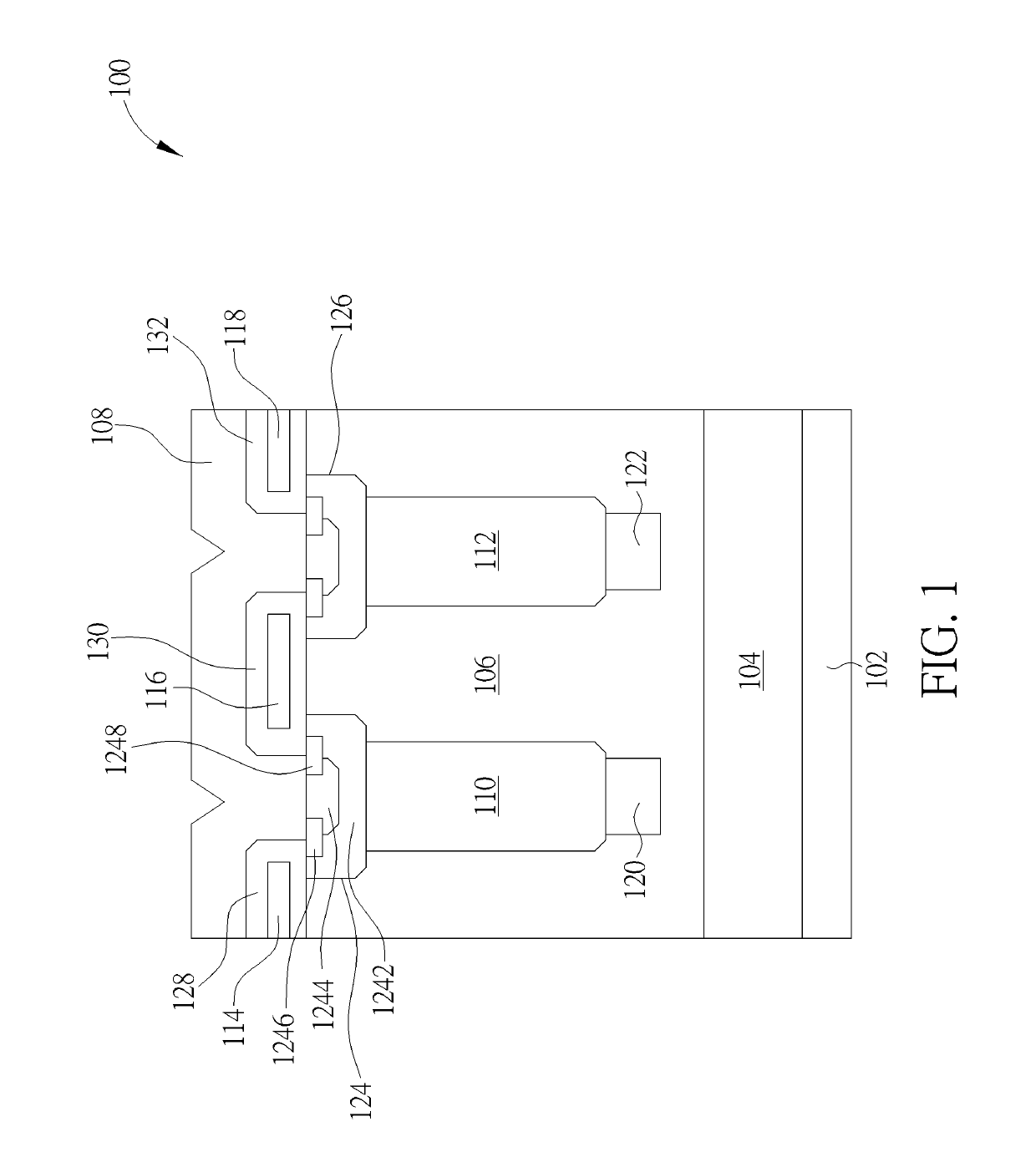
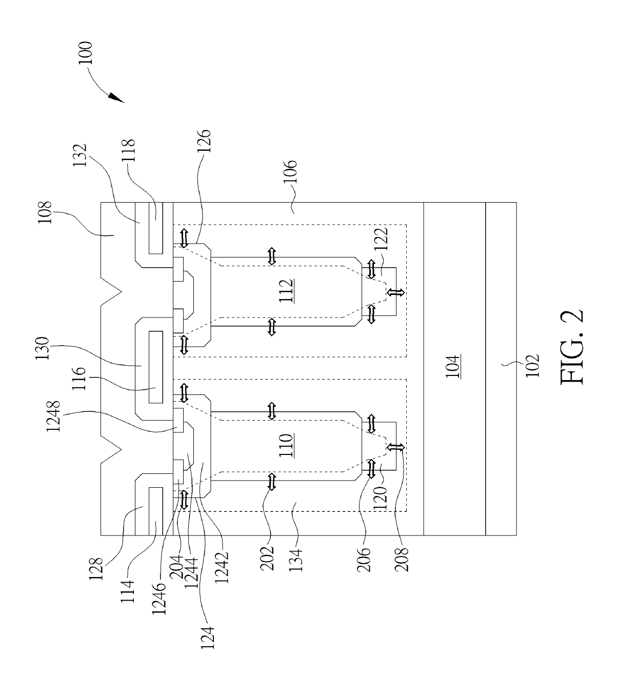
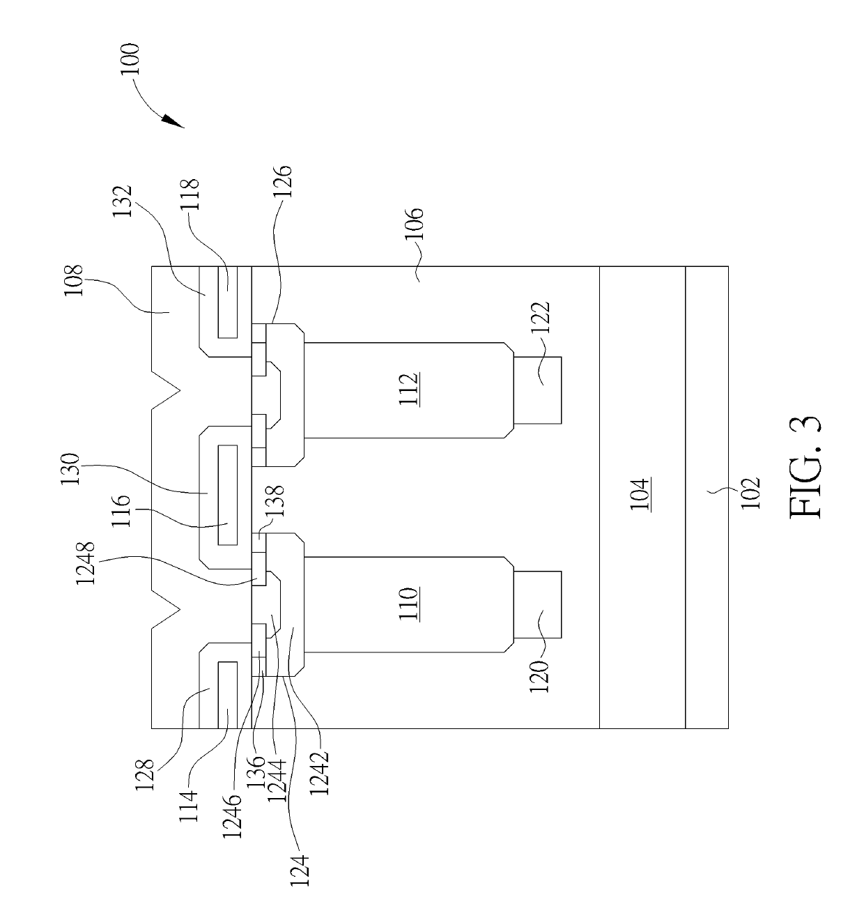
[0017]Please refer to FIG. 1. FIG. 1 is a diagram illustrating a power metal-oxide-semiconductor field-effect transistor (MOSFET) device 100 with three-dimensional super junction according to the present invention. As shown in FIG. 1, the power MOSFET device 100 includes a first metal layer 102, a substrate 104, an epitaxy layer 106, and a second metal layer 108. In addition, FIG. 1 only further shows first trench wells 110, 112 of a plurality of first trench wells of the power MOSFET device 100, polysilicon layers 114, 116, 118 of a plurality of polysilicon layers of the power MOSFET device 100, second trench wells 120, 122 of a plurality of second trench wells of the power MOSFET device 100, and body structure layers 124, 126 of a plurality of body structure layers of the power MOSFET device100, wherein the substrate 104 and the epitaxy layer 106 has a first conductivity type, the plurality of first trench wells and the plurality of second trench wells has a second conductivity ty...

second embodiment

[0021]Please refer to FIG. 4. FIG. 4 is a diagram illustrating a power MOSFET device 400 with three-dimensional super junction according to the present invention. As shown in FIG. 4, a difference between the power MOSFET device 400 and the power MOSFET device 100 is that each first trench well (e.g. first trench wells 410, 412) of the power MOSFET device 400 and an epitaxy layer 406 are generated by a multi-epitaxy & ion implantation method, wherein ion doping concentration and widths of trench layers 4102-4108 of the first trench well 410 can be identical or different. For example, in one embodiment of the present invention, ion doping concentration of the trench layers 4102-4108 is gradually increased from top to bottom and widths of the trench layers 4102-4108 are identical (as shown in FIG. 4). In addition, in another embodiment of the present invention, the ion doping concentration of the trench layers 4102-4108 is gradually increased from top to bottom and the widths of the tr...

third embodiment

[0023]Please refer to FIGS. 2, 9, 10. FIG. 9 is a flowchart illustrating a fabrication method of a power MOSFET device with three-dimensional super junction according to the present invention. The fabrication method in FIG. 9 is illustrated using FIG. 10. Detailed steps are as follows:

[0024]Step 900: Start.

[0025]Step 902: The substrate 104 is formed on the first metal layer 102.

[0026]Step 904: The epitaxy layer 106 is formed on the substrate 104.

[0027]Step 906: The plurality of second trenches are formed in the epitaxy layer 106.

[0028]Step 908: A second epitaxy with the second conductivity type is filled to the plurality of second trenches to form the plurality of second trench wells.

[0029]Step 910: The epitaxy layer 106 is deposited again.

[0030]Step 912: The plurality of first trenches are formed in the epitaxy layer 106.

[0031]Step 914: A first epitaxy with the second conductivity type is filled to the plurality of first trenches to form the plurality of first trench wells.

[0032]St...


PUM


Abstract

A power metal-oxide-semiconductor field-effect transistor (MOSFET) device includes a first metal layer, a substrate, an epitaxy layer, a plurality of first trench wells, a plurality of second trench wells, a plurality of body structure layers, a plurality of polysilicon layers, and a second metal layer. A part of a depletion region is formed between each first trench well and the epitaxy layer and between a body structure layer corresponding to the each first trench well and the epitaxy layer, and a rest part of the depletion region is formed between a second trench well corresponding to the each first trench well and the epitaxy layer. The plurality of second trench wells increase a breakdown voltage of the power MOSFET device and reduce a conduction resistor of the power MOSFET device.

Description

BACKGROUND OF THE INVENTION1. Field of the Invention[0001]The present invention relates to a power metal-oxide-semiconductor field-effect transistor (MOSFET) device with three-dimensional super junction and a fabrication method thereof, and particularly to a power MOSFET device and a fabrication method thereof that can increase a breakdown voltage of the power MOSFET device and reduce a conduction resistor of the power MOSFET device.2. Description of the Prior Art[0002]In the prior art, when a power metal-oxide-semiconductor field-effect transistor (MOSFET) device with three-dimensional super junction is turned off, the power MOSFET device utilizes a PN junction between a P-well and an N type epitaxy layer of the power MOSFET device to form a depletion region to endure a voltage between a drain and a source of the power MOSFET device. When a width of the depletion region is increased, the voltage between the drain and the source of the power MOSFET device endured by the depletion re...

Claims


Application Information

Patent Timeline
Patent Type & Authority Patents(United States)
IPC IPC(8): H01L29/06H01L21/265H01L29/66H01L21/02H01L29/10H01L29/78
CPCH01L29/0634H01L21/02634H01L21/265H01L29/1095H01L29/66712H01L29/7802
Inventor HSIUNG, CHIH-WENYEH, JEN-HAOTU, YI-RONGTSENG, WAN-WEN
Owner LEADTREND TECH
Why Eureka
Try Eureka