Insulated gate switching element and method of controlling the insulated gate switching element

a technology of insulating gate and insulating layer, which is applied in the direction of electronic switching, pulse technique, semiconductor devices, etc., can solve the problems of difficult to reduce the distance between an emitter region and a drift region, and difficult to reduce the channel length to a predetermined length or shorter, so as to reduce the effective channel length, increase the thickness of the channel, reduce the effect of the surface layer portion

Inactive Publication Date: 2016-10-27
TOYOTA JIDOSHA KK
View PDF0 Cites 0 Cited by
  • Summary
  • Abstract
  • Description
  • Claims
  • Application Information

AI Technical Summary

Benefits of technology

[0009]In the insulated gate switching element according to the aspect, when a gate voltage is applied, a channel is formed in the main base region and the surface layer base region which face a gate electrode. When the gate voltage is increased, the thickness of the channel is increased. When the thickness of the channel in the surface layer base region reaches the thickness of the surface layer base region, the first semiconductor region and the second semiconductor region are connected to each other through the channel. When the first semiconductor region and the second semiconductor region are connected to each other through the channel, current flows between the first semiconductor region and the second semiconductor region. That is, the insulated gate switching element is turned on. Since the second semiconductor region comes into contact with the surface layer base region on the rear surface side, current flows primarily in a vertical direction (the thickness direction of the semiconductor substrate) between the second semiconductor region and the surface layer base region. Therefore, a portion of the channel (that is, the gate insulating film) in which the current flows is primarily the channel in the surface layer portion of the main base region. Therefore, the length of the surface layer portion of the main base region (that is, the distance between the first semiconductor region and the surface layer base region) is an effective channel length. Therefore, by reducing the length of the surface layer portion of the main base region, the effective channel length can be reduced, thereby reducing the on-resistance of the insulated gate switching element. In addition, the second semiconductor region is connected to the surface layer portion of the main base region through the surface layer base region. That is, the second semiconductor region does not directly come into contact with the surface layer portion of the main base region. Therefore, the extension of a depletion layer to the surface layer portion from the second semiconductor region can be suppressed. Accordingly, a short-channel effect can be suppressed. Therefore, in the insulated gate switching element, even when the effective channel length (the length of the surface layer portion of the main base region) is reduced, the short-channel effect is less likely to occur, and the gate threshold is less likely to decrease. Therefore, according to the structure of the insulated gate switching element, a high gate threshold and a low on-resistance can be compatible with each other.

Problems solved by technology

Due to the occurrence of the short-channel effect, it is difficult to reduce the channel length of the MOSFET to a predetermined length or shorter.
Similarly, even in an insulated-gate bipolar transistor (IGBT), it is difficult to reduce the channel length (that is, the distance between an emitter region and a drift region) to a predetermined length or shorter due to the short-channel effect.
As described above, in an insulated gate switching element according to the related art, due to the occurrence of the short-channel effect, it is difficult to reduce an on-resistance while maintaining a high gate threshold.

Method used


Image

  • Insulated gate switching element and method of controlling the insulated gate switching element
  • Insulated gate switching element and method of controlling the insulated gate switching element
  • Insulated gate switching element and method of controlling the insulated gate switching element

Examples


Embodiment Construction

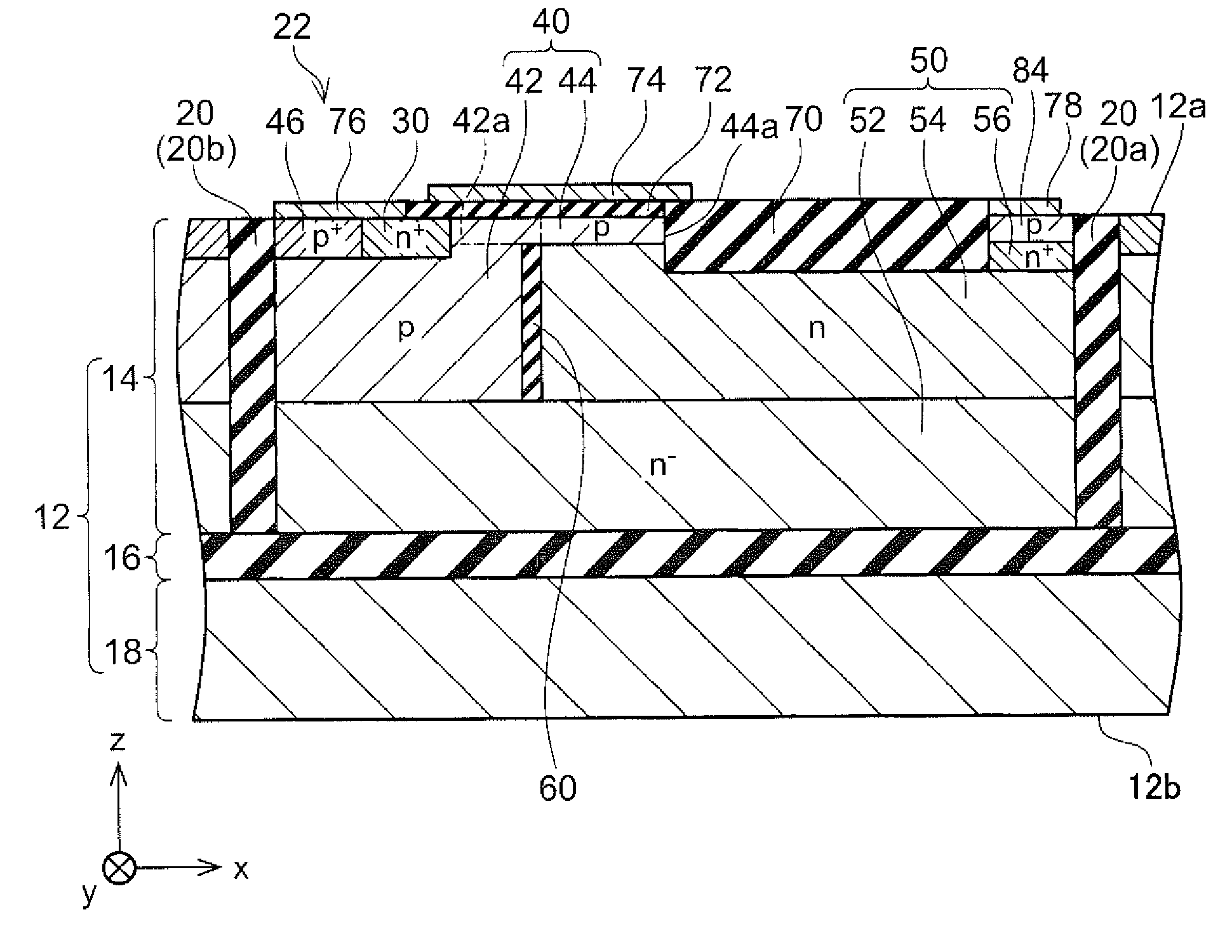
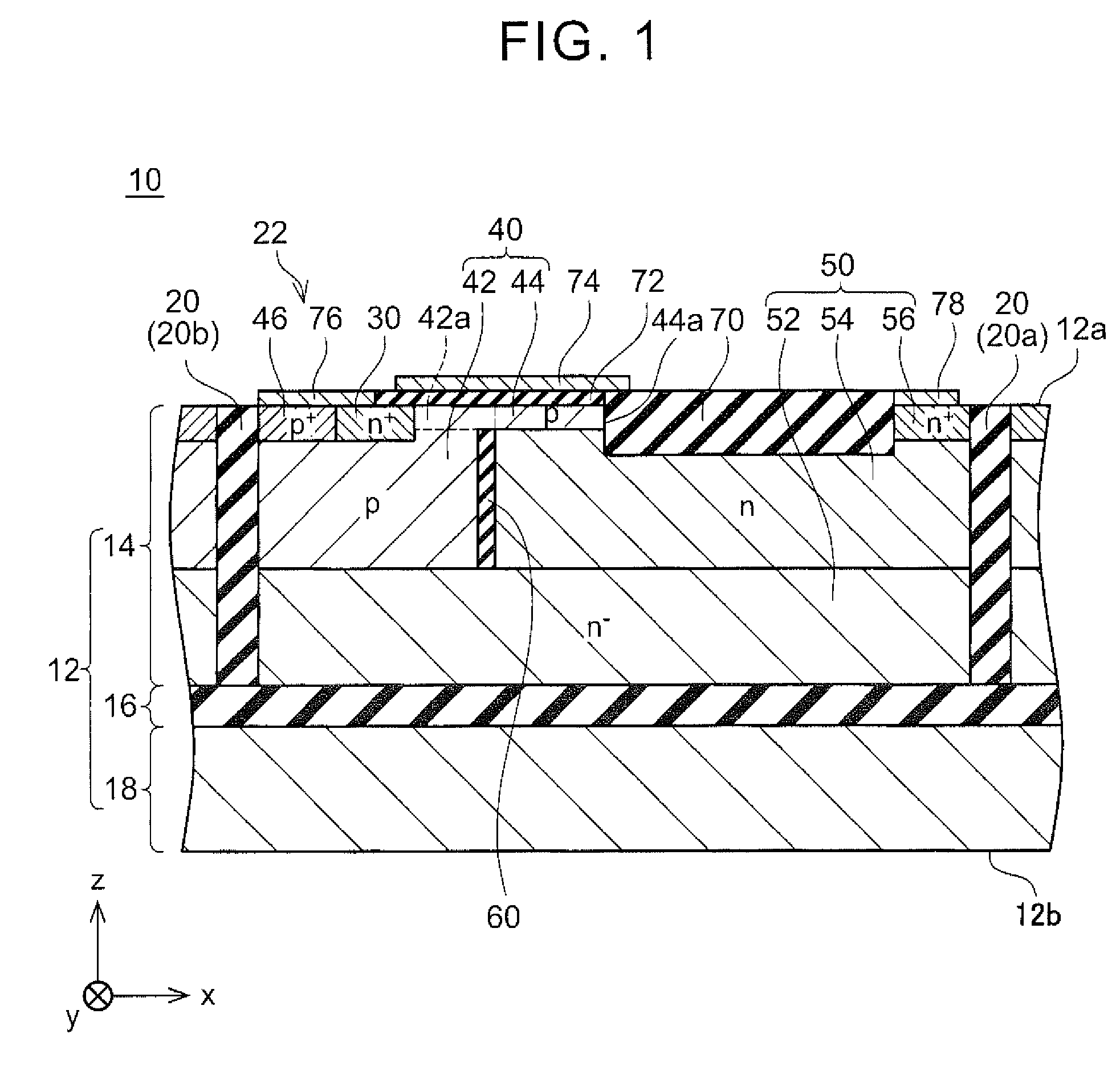
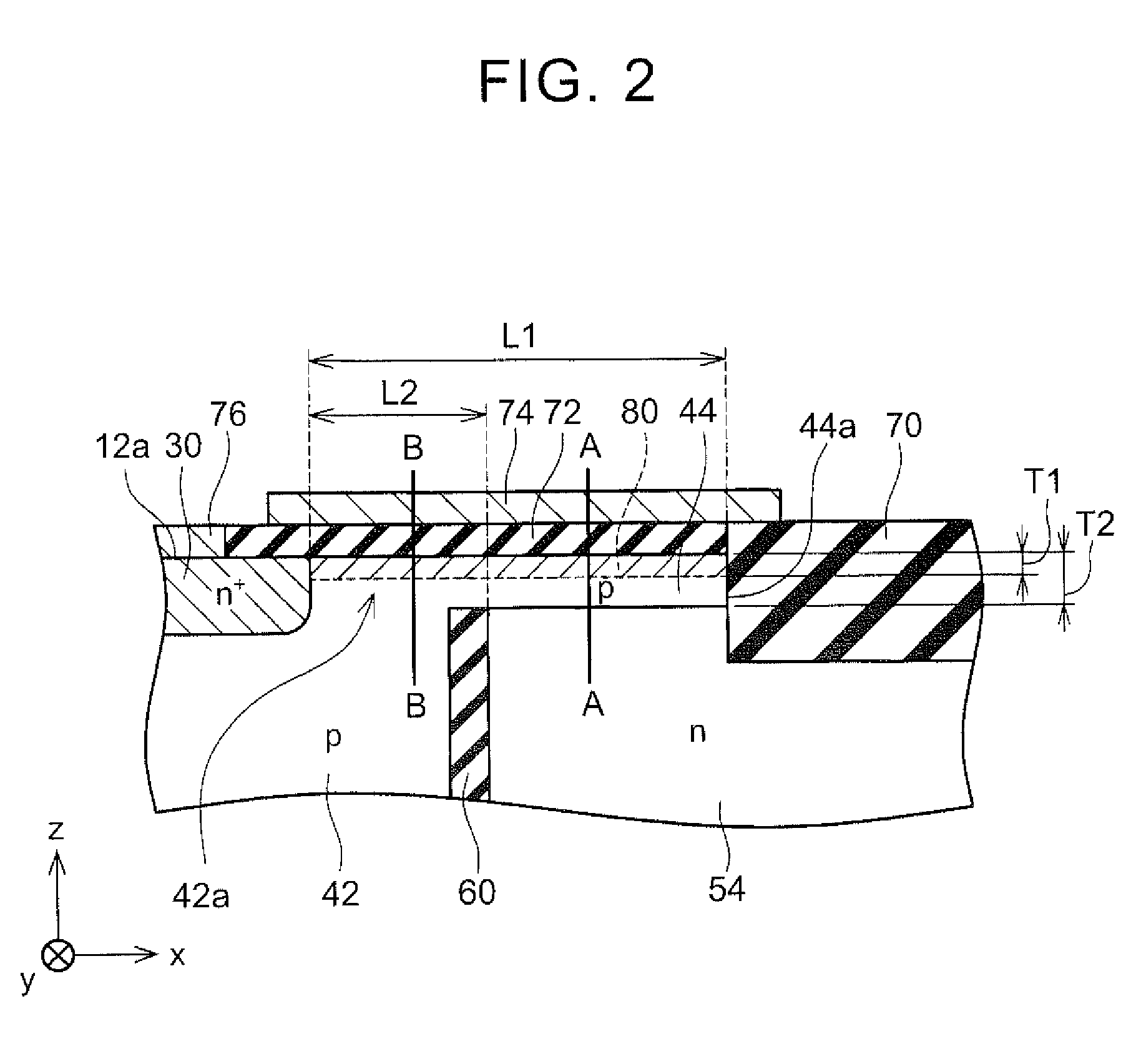
[0030]A MOSFET 10 of Example 1 illustrated in FIG. 1 is an n-channel MOSFET. The MOSFET 10 includes a silicon on insulator (SOI) substrate 12. In the following description, a direction parallel to a surface 12a of the SOI substrate 12 (rightward and leftward directions in FIG. 1) is referred to as an x direction, a direction that is parallel to the surface 12a and is perpendicular to the x direction is referred to as a y direction, and a thickness direction of the SOI substrate 12 is referred to as a z direction. The SOI substrate 12 includes a handle layer 18, a box layer 16, and a device layer 14. The handle layer 18 is formed of single-crystal silicon. The handle layer 18 is exposed at a rear surface 12b of the SOI substrate 12. The box layer 16 is formed of silicon oxide. The box layer 16 is laminated on the handle layer 18. The device layer 14 is formed of single-crystal silicon. The device layer 14 is laminated on the box layer 16. The device layer 14 is insulated from the han...


PUM


Abstract

A semiconductor substrate includes: a first conduction type first semiconductor region exposed at a first surface; a second conduction type main base region exposed at the first surface at a position adjacent to the first semiconductor region; and a second conduction type surface layer base region which is exposed at the first surface at a position adjacent to the main base region and has a smaller thickness than that of the main base region. A gate electrode is disposed across upper portions of the first semiconductor region, the main base region, and the surface layer base region.

Description

INCORPORATION BY REFERENCE[0001]The disclosure of Japanese Patent Application No. 2015-087749 filed on Apr. 22, 2015 including the specification, drawings and abstract is incorporated herein by reference in its entirety.BACKGROUND OF THE INVENTION[0002]1. Field of the Invention[0003]The invention relates to an insulated gate switching element and a method of controlling the insulated gate switching element.[0004]2. Description of Related Art[0005]Japanese Patent Application Publication No. 2011-187853 (JP 2011-187853 A) discloses a metal-oxide-semiconductor field-effect transistor (MOSFET). When a voltage of a threshold or higher is applied to a gate electrode of the MOSFET, a channel is formed in a base region. Therefore, carriers flow from a source region toward a drain region through the channel. That is the MOSFET is turned on. When the voltage applied to the gate electrode is reduced to be lower than the threshold, the channel disappears and the flow of the carriers is stopped....

Claims


Application Information

Patent Timeline
Patent Type & Authority Applications(United States)
IPC IPC(8): H01L29/10H03K17/567H01L29/78H01L29/06H01L29/739
CPCH01L29/1095H01L29/0649H03K17/567H01L29/7816H01L29/7394H01L29/0646H01L29/0653H01L29/0878H01L29/42368H01L29/7824
Inventor ISHIDA, TAKASHIOKAWA, TAKASHI
Owner TOYOTA JIDOSHA KK
Why Eureka
Try Eureka