Light emitting device including light emitting element, outer connection electrodes and resin layer

a light emitting device and outer connection electrode technology, applied in semiconductor devices, semiconductor/solid-state device details, electrical apparatus, etc., can solve problems such as self alignment problems in relation to csp, and achieve the effect of effectively preventing self alignment problems

Active Publication Date: 2016-03-22
CITIZEN WATCH CO LTD +2
View PDF7 Cites 21 Cited by
  • Summary
  • Abstract
  • Description
  • Claims
  • Application Information

AI Technical Summary

Benefits of technology

[0008]The present invention is proposed in light of the above problems, and has the object of providing a light emitting device that enables effective prevention of self alignment problems resulting from a joint material between the mounting substrate and the CSP electrode or as a result of the type and condition of the mounting substrate.
[0020]With the light emitting device of the present invention, it is possible to effectively prevent self alignment problems resulting from a joint material between the mounting substrate and the CSP electrode or as a result of the type and condition of the mounting substrate.

Problems solved by technology

However, self alignment problems have arisen in relation to CSP due to the type and condition of the mounting substrate provided for mounting the light emitting device or the type of the joint material that is joined to the electrode that is disposed on the CSP surface.

Method used


Image

  • Light emitting device including light emitting element, outer connection electrodes and resin layer
  • Light emitting device including light emitting element, outer connection electrodes and resin layer
  • Light emitting device including light emitting element, outer connection electrodes and resin layer

Examples


first embodiment

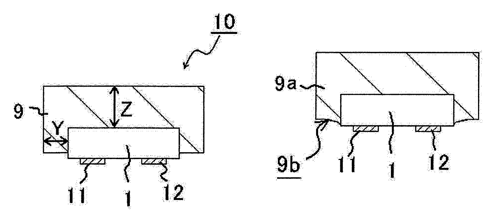
[0036]As illustrated in FIG. 1A, the light emitting device 10 according to this embodiment includes a light emitting element 1, a first outer connection electrode 11 and a second outer connection electrode 12 that are respectively connected to a first electrode and a second electrode of the light emitting element 1 as described below, and a resin layer 9 that is configured to cover the lower surface and side surface of the light emitting element 1. The upper surface of the resin layer 9 is disposed at a position that is lower than the upper surface of a semiconductor laminated body.

[0037]The light emitting device normally has a planar configuration in the shape of a rectangle or substantially in the shape of a rectangle. As used herein, “substantially in the shape of a rectangle” means that a fluctuation is allowed in the angle of the four corners of 90±10 degrees.

[Light Emitting Element]

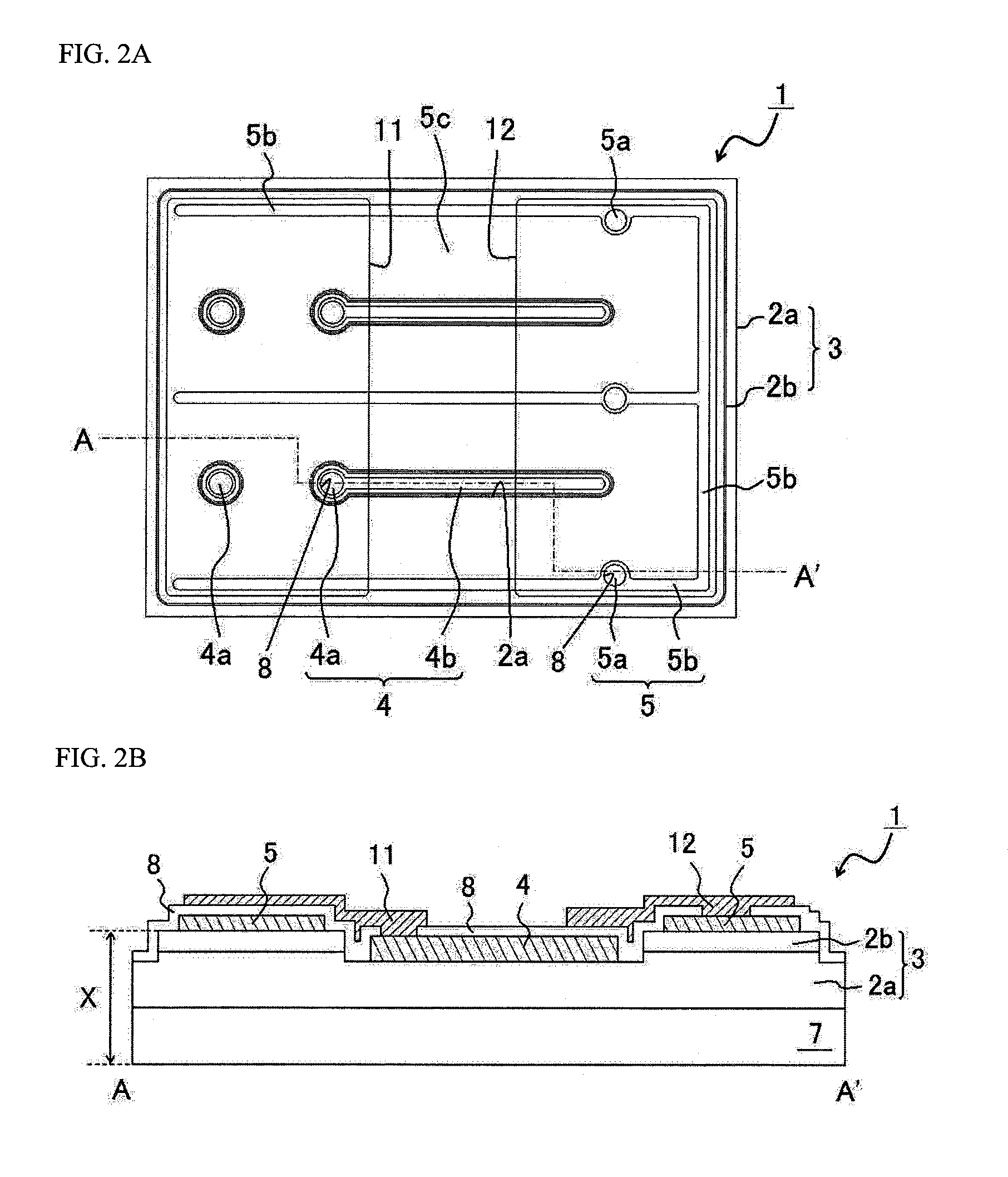
[0038]As illustrated in FIG. 2A and FIG. 2B, the light emitting element 1 has a semiconductor la...

second embodiment

[0074]As illustrated in FIG. 4A, the light emitting device 20 according to this embodiment includes a second resin layer 18 that contains a fluorescent material on the lower surface of the of the light emitting element 1 in addition to the resin layer 19 on the side surface of the light emitting element 1, and in other respects has the substantially the same configuration as the light emitting device 10 according to the first embodiment.

[0075]The resin layer 19 may expose a portion of the side surface of the semiconductor laminated body 3 (reference is made to FIG. 4A), or although the side surface of the semiconductor laminated body 3 is covered, the upper surface 19b of the resin layer 19a may become gradually lower in accordance with separation from the semiconductor laminated body 3 (reference is made to FIG. 4B).

[0076]The resin layer 19 and the second resin layer 18 may be formed by the following method.

[0077]As illustrated in FIG. 5A, the light emitting element 1 is adhere to ...

third embodiment

[0082]As illustrated in FIG. 6A and FIG. 6B, the light emitting device according to the present embodiment has a different structure in relation to the first electrode 34 and the second electrode 35 of the light emitting element as described below, and in other respects has the substantially the same configuration as the light emitting device 10 according to the first embodiment.

[0083]An insulating film 38 may be disposed between the first outer electrode 11 and the second outer electrode 12 on the lower surface of the light emitting device. The disposition of the insulating film 38 enables prevention of an electrical connection between those two electrodes. Furthermore, a short circuit connection can be prevented in relation to both outer electrodes of the joint material during mounting operations.

(First Electrode and Second Electrode)

[0084]The first electrode 34 and the second electrode 35 of the light emitting device 31 includes a first ohmic electrode 34a and a second ohmic elec...


PUM


Abstract

A semiconductor device has a light emitting element, and a resin layer; the light emitting element includes a semiconductor laminated body in which a first semiconductor layer and a second semiconductor layer are laminated in sequence, a second electrode connected to the second semiconductor layer on an upper surface of the second semiconductor layer that forms an upper surface of the semiconductor laminated body, and a first electrode connected to the first semiconductor layer on an upper surface of the first semiconductor layer in which a portion of the second semiconductor layer on one surface of the semiconductor laminated body is removed and a portion of the first semiconductor layer is exposed; and the resin layer is configured to cover at least a side surface of the light emitting element, and an upper surface of the resin layer is lower than the upper surface of the semiconductor laminated body.

Description

CROSS-REFERENCE TO RELATED APPLICATIONS[0001]This application claims priority to Japanese Patent Application No. 2013-024746 filed on Feb. 12, 2013. The entire disclosure of Japanese Patent Application No. 2013-024746 is hereby incorporated herein by reference.BACKGROUND[0002]1. Technical Field[0003]The disclosure relates to a light emitting device, and in particular to the electrode structure of a light emitting device.[0004]2. Related Art[0005]In recent years, various light emitting devices using a light emitting element that is enlarged to at least 1 mm×(0.5 to 1) mm have been developed in response to increasing developments of high-intensity brightness. A light emitting device using this type of light emitting element has a planar size that is equivalent to the light emitting element, is termed a chip size package (CSP), and is configured so that the electrodes that are used for mounting are disposed on the surface. The number that is provided on the package substrate in respons...

Claims


Application Information

Patent Timeline
Patent Type & Authority Patents(United States)
IPC IPC(8): H01L33/62H01L33/54H01L33/38H01L33/50H01L23/00H01L33/46
CPCH01L24/96H01L33/38H01L33/505H01L33/54H01L33/62H01L33/382H01L33/46H01L2924/12036H01L2924/181H01L2924/00H01L2224/04105H01L2924/3511
Inventor KUSUSE, TAKESHIOGAWA, TOSHIAKIMINATO, SHUNSUKEOYAMADA, NODOKA
Owner CITIZEN WATCH CO LTD
Why Eureka
Try Eureka