Carbon nanotube field-effect transistor encoder

a technology of carbon nanotube and encoder, which is applied in the field of encoders, can solve the problems of weakening performance, changing stability, and defects of cmos technology, and achieves the effects of simple circuit structure, lower cost and power consumption, and higher integration level

Active Publication Date: 2016-03-22
NINGBO UNIV
View PDF3 Cites 0 Cited by
  • Summary
  • Abstract
  • Description
  • Claims
  • Application Information

AI Technical Summary

Benefits of technology

[0008]In view of the above-described problems, it is one objective of the invention to provide a carbon nanotube field-effect transistor encoder which has the simple circuit structure, higher integration level and lower cost and power consumption.
[0012]Compared to prior art, the invention has the advantages of that, on the basis of the binary circuit which comprises a first inverter, a second inverter, a third inverter, a first three-input NAND gate, a second three-input NAND gate, a third three-input NAND gate, a fourth three-input NAND gate, a fifth three-input NAND gate, a sixth three-input NAND gate, a seventh three-input NAND gate, a first two-input NAND gate, a second two-input NAND gate, a third two-input NAND gate and a two-input AND gate, when the input end of the encoder inputs three-bit binary input signals, the three-bit binary input signals are first processed by the binary circuit; and the processed signals are input into the ternary circuit which comprises a first CNFET NAND gate, a second CNFET NAND gate, a first CNFET NOR gate, a second CNFET NOR gate, a fourth inverter and a fifth inverter to be converted into ternary signals for transmission. Therefore, the encoder of the invention converts three-bit binary signals into two-bit ternary signals by a binary and ternary hybrid circuit, which not only reduces the amount of leads for external signals in the circuit but also is compatible with existing binary circuits. The circuit has the simple structure, the higher integration level and the lower cost and power consumption.

Problems solved by technology

With the improving integration level of chips and the reducing technological feature size, defects of the CMOS technology also become obvious, for example, the increment of leakage current, weakening performance and change stability.
Therefore, the wiring area of encoder circuits increases, the structure of circuits is complex and the power consumption is large.

Method used


Image

  • Carbon nanotube field-effect transistor encoder
  • Carbon nanotube field-effect transistor encoder
  • Carbon nanotube field-effect transistor encoder

Examples


example 1

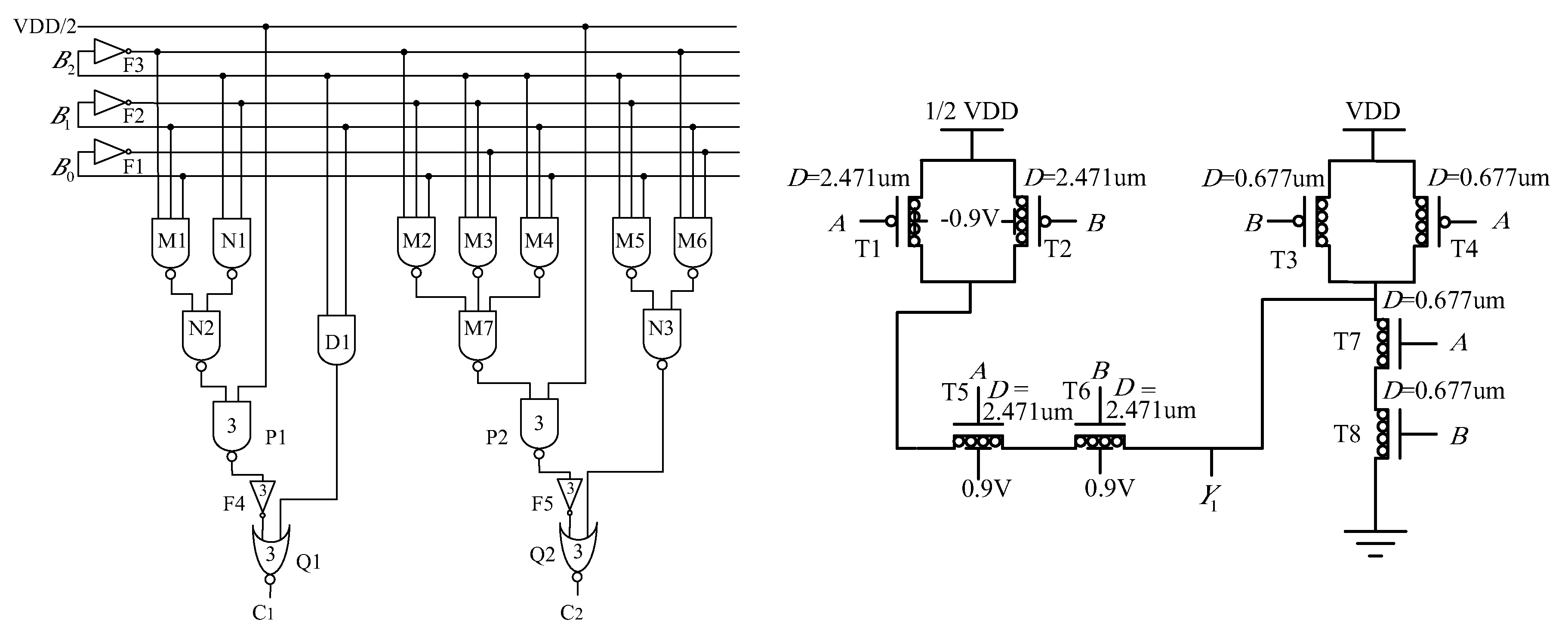
[0022]As shown in FIG. 1, a carbon nanotube field-effect transistor encoder comprises a first inverter F1, a second inverter F2, a third inverter F3, a fourth inverter F4, a fifth inverter F5, a first three-input NAND gate M1, a second three-input NAND gate M2, a third three-input NAND gate M3, a fourth three-input NAND gate M4, a fifth three-input NAND gate M5, a sixth three-input NAND gate M6, a seventh three-input NAND gate M7, a first two-input NAND gate N1, a second two-input NAND gate N2, a third two-input NAND gate N3, a two-input AND gate, a first CNFET NAND gate P1, a second CNFET NAND gate P2, a first CNFET NOR gate Q1 and a second CNFET NOR gate Q2; the input end of the first inverter F1, the first input end of the first three-input NAND gate M1, the first input end of the second three-input NAND gate M2, the first input end of the fourth three-input NAND gate M4 and the first input end of the fifth three-input NAND gate M5 connect, and the connecting end is the first inp...

example 2

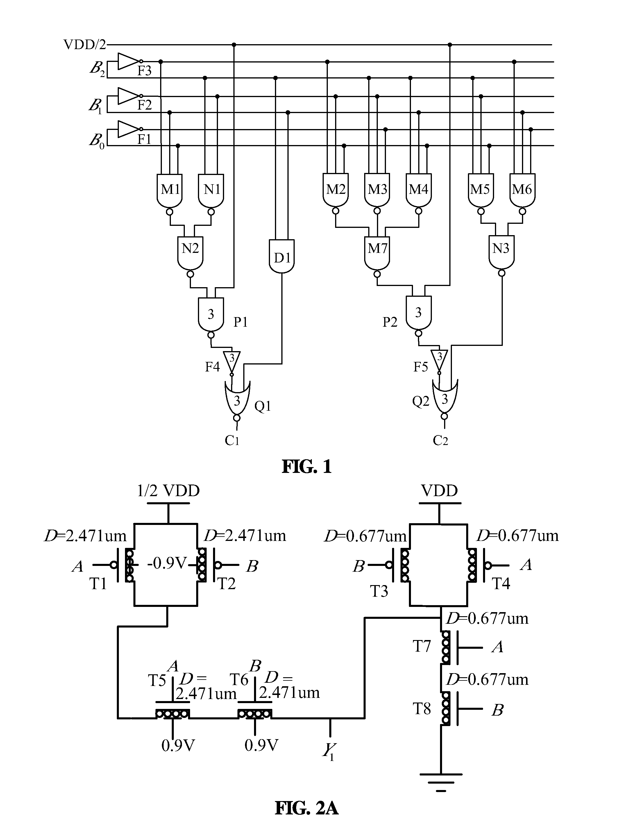
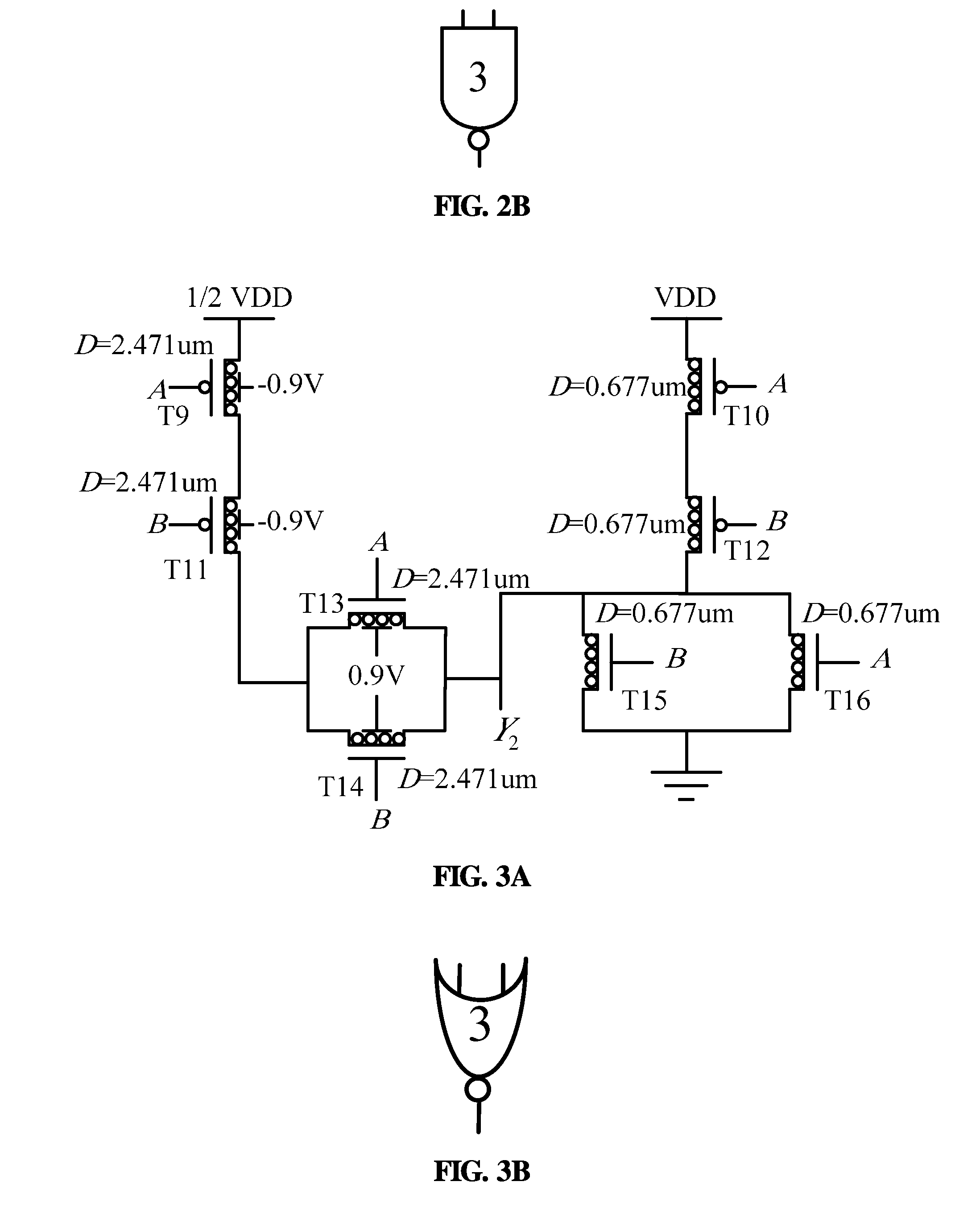
[0031]Example 1 and Example 2 are basically identical. The difference is just that, in Example 2, the first CNFET NAND gate P1, the second CNFET NAND gate P2, the first CNFET NOR gate Q1 and the second CNFET NOR Q2 adopt the ternary NAND and NOR circuits which are disclosed in the literature Moaiyeri M H, Doostaregan A, Navi K. Design of Energy-efficient and Robust Ternary Circuits for Nanotechnology [J]. Circuits, Devices & Systems, IET, 2011, 5(4): 285-296. The ternary NAND and NOR circuits in the literature make the logic outputs of NTI and PTI string together through two CNFETs to get standard logic NAND and NOR gates.

[0032]Under the condition of the same technological parameters, when the load capacitance is 10 fF, the energy consumption comparison is conducted between the encoder of Example 1 and the encoder of Example 2, and the comparison diagram of the energy consumption of the encoders is shown in FIG. 5. According to the analysis of FIG. 5, compared to the encoder in Exam...


PUM

PropertyMeasurementUnit
voltageaaaaaaaaaa
voltageaaaaaaaaaa
load capacitanceaaaaaaaaaa

Abstract

A carbon nanotube field-effect transistor encoder, based on a binary circuit which includes: a first inverter, a second inverter, a third inverter, a first three-input NAND gate, a second three-input NAND gate, a third three-input NAND gate, a fourth three-input NAND gate, a fifth three-input NAND gate, a sixth three-input NAND gate, a seventh three-input NAND gate, a first two-input NAND gate, a second two-input NAND gate, a third two-input NAND gate and a two-input AND gate. When the input end of the encoder inputs three-bit binary input signals, the three-bit binary input signals are first processed by the binary circuit; and the processed signals are input into the ternary circuit which includes a first CNFET NAND gate, a second CNFET NAND gate, a first CNFET NOR gate, a second CNFET NOR gate, a fourth inverter and a fifth inverter to be converted into ternary signals for transmission.

Description

CROSS-REFERENCE TO RELATED APPLICATIONS[0001]Pursuant to 35 U.S.C. §119 and the Paris Convention Treaty, this application claims the benefit of Chinese Patent Application No. 201410089615.6 filed Mar. 12, 2014, the contents of which are incorporated herein by reference. Inquiries from the public to applicants or assignees concerning this document or the related applications should be directed to: Matthias Scholl P. C., Attn.: Dr. Matthias Scholl Esq., 245 First Street, 18th Floor, Cambridge, Mass. 02142.BACKGROUND OF THE INVENTION[0002]1. Field of the Invention[0003]The invention relates to an encoder, in particular to a carbon nanotube field-effect transistor encoder.[0004]2. Description of the Related Art[0005]An encoder is a combinational logic circuit for realizing conversion between different digitals. Due to the high precision, high resolution and high reliability of encoders, encoders are widely used in various encoding operations in industrial automation. At present, integra...

Claims


Application Information

Patent Timeline
Patent Type & Authority Patents(United States)
IPC IPC(8): H03K19/00H03K19/20H03K19/094
CPCH03K19/0013H03K19/09425H03K19/20
Inventor WANG, PENGJUNTANG, WEITONGWANG, QIAN
Owner NINGBO UNIV
Why Eureka
Try Eureka