Method for preparing graphene nanoribbon on insulating substrate

a graphene nanoribbon and substrate technology, applied in the direction of graphene nanoribbons, solid-state diffusion coatings, transportation and packaging, etc., can solve the problems of reducing the electron mobility of graphene, high temperature required for sic pyrolysis, and high cost of sic substrates

Active Publication Date: 2016-05-03
SHANGHAI INST OF MICROSYSTEM & INFORMATION TECH CHINESE ACAD OF SCI
View PDF3 Cites 2 Cited by
  • Summary
  • Abstract
  • Description
  • Claims
  • Application Information

AI Technical Summary

Benefits of technology

[0022]Cleavage of the hBN substrate is to remove a top layer of hBN by a mechanical stripping method, and meanwhile, surface adsorbates and defects, such as a surface mechanical scratch, are eliminated, so that a fresh hBN atomic surface is exposed with few surface defects.
[0023]Preferably, in the mixture of the hydrogen gas and the argon gas, a volume ratio of the hydrogen gas and the argon gas is from 1:1 to 1:10, and preferably from 1:2 to 1:9. An annealing temperature of the high-temperature annealing treatment is from 1,000° C. to 1,200° C., and an annealing time thereof is from 10 min to 300 min. The annealing temperature may regulate and control an etching rate, and the annealing time may regulate and control distribution of the single atomic steps.
[0032]In the present invention, the substrate having steps of the thickness of a single atomic layer is used as a base to control a graphene deposition technology and grow the graphene nanoribbon in a step-flow mode. In a growth and nucleation process of the graphene, nucleation energy required for the nucleation on a defect portion, especially, a portion below the step is smaller than that on the plane, so that the single atomic step on the insulating substrate can become a nucleation zone for the growth of the graphene. By using a difference between nucleation energy at a step edge and that on the plane, and by controlling the temperature, the intensity of pressure and the supersaturation degree of activated carbon atoms in the growth process, the nucleation may be controlled to only occur at the atomic step, thereby achieving the effect of growing a graphene nanoribbon.
[0033]In the present invention, preparation technologies compatible with a semiconductor technology, such as the LPCVD, the PECVD, and the PLD are used for implementing the graphene nanoribbon on the insulating substrate, which avoids the transfer of the graphene, and the substrate with atomic level flatness ensures the performance of the prepared graphene. The prepared graphene nanoribbon may be directly used to prepare a graphene electronic device.

Problems solved by technology

The temperature required for the SiC pyrolysis is too high, which is not compatible with a current semiconductor technology, and the cost of a SiC substrate is also high.
However, currently, when preparing graphene on a transition metal, the prepared graphene needs to be transferred onto an insulating substrate.
A wet chemical process is used in the transfer process, and a defect is unavoidably introduced, which greatly lowers the electron mobility of the graphene.
A SiO2 / Si substrate is not a suitable or first-choice substrate for a graphene electronic device.
However, the graphene prepared by this method completely coats the hBN substrate, and meanwhile, the controllability of the thickness is not sufficient, making it difficult to implement uniform single-layered and double-layered graphene.
An article “Direct graphene growth on insulator” written by G. Lippert, et al. puts forward a method for growing graphene on a mica surface by an MBE method, but the obtained graphene is of poor quality.
Currently, direct growth of the graphene on the hBN is far from meeting the requirement for preparing a chip.
The feature size and thickness of the graphene nanoribbons prepared by the two methods are in a certain range, and are difficult to be precisely controlled.
Currently, it is not implemented that the CVD or another deposition means is directly used to grow a high-quality graphene nanoribbon on an insulating substrate which meets a microelectronic requirement.

Method used


Image

  • Method for preparing graphene nanoribbon on insulating substrate
  • Method for preparing graphene nanoribbon on insulating substrate
  • Method for preparing graphene nanoribbon on insulating substrate

Examples


embodiment 1

Preparation of an hBN Substrate Having Single Atomic Layer Steps

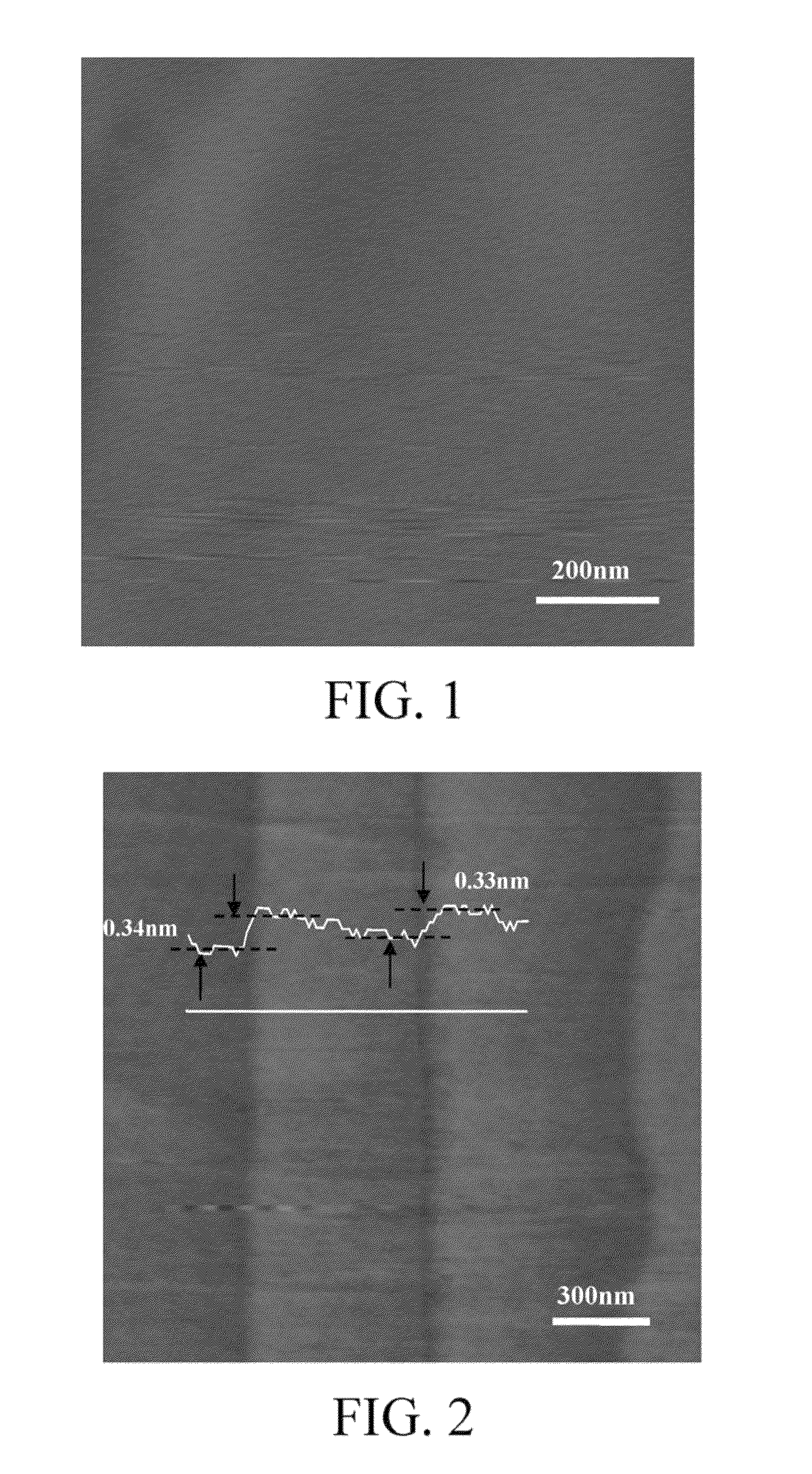
[0046]Step 1: Use a monocrystal hBN flake as a raw material, and mechanically strip the monocrystal hBN flake on a SiO2 / Si substrate to obtain an hBN sheet having a fresh cleavage plane, and as shown in FIG. 1, a surface thereof is highly flat without any step.

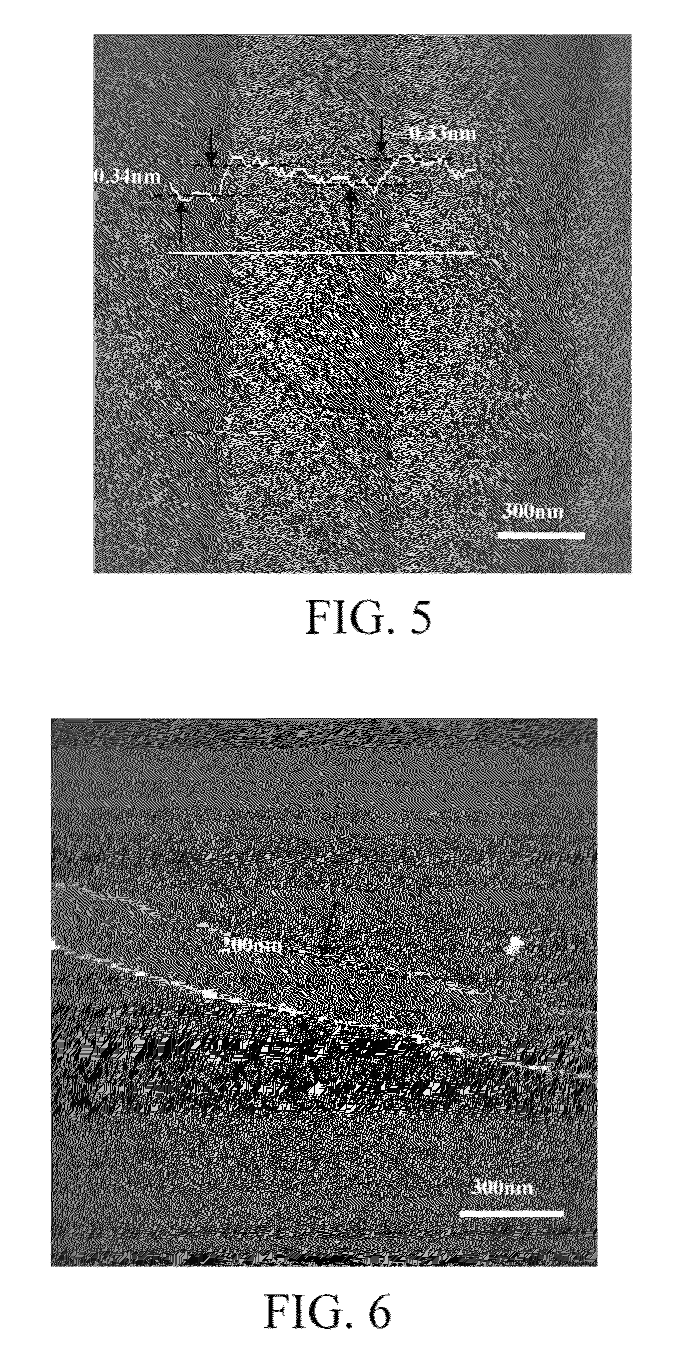
[0047]Step 2: Put an hBN / SiO2 substrate obtained in Step 1 into a tube furnace, feed therein 300 sccm of a mixture of hydrogen gas and argon gas (a volume ratio thereof is H2:Ar=1:3), heat the temperature up to 1,200° C. at a rate of 20° C. / min, maintain the temperature unchanged for 10 min, and allow to cool down with the tube furnace. In this way, steps having the height of a single atomic layer as shown in FIG. 2 are obtained. As is shown by a height analysis, height differences of the steps are 0.34 nm and 0.33 nm, the steps are steps of a single BN atomic layer, and a spacing between the steps is about 500 nm.

embodiment 2

Preparation of an hBN Substrate Having Single Atomic Layer Steps

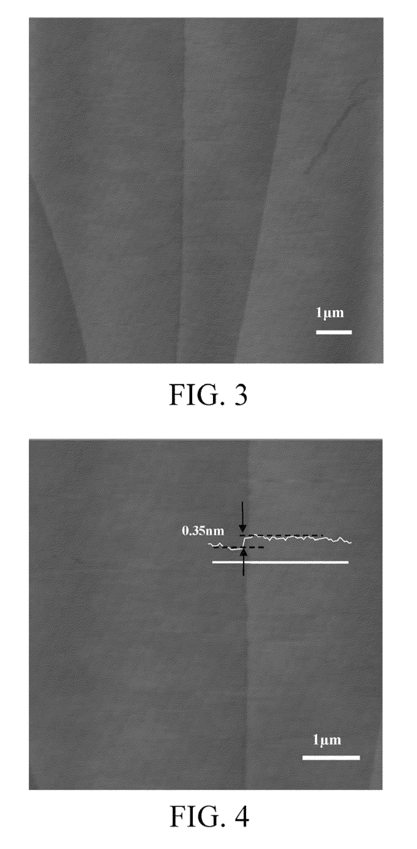
[0048]Step 1: Use a monocrystal hBN bulk as a substrate, and remove a surface layer of hBN by using a mechanical stripping method.

[0049]Step 2: Put the substrate into a tube furnace, feed therein 300 sccm of a mixture of hydrogen gas and argon gas (a volume ratio thereof is H2:Ar=1:6), heat the temperature up to 1,100° C. at a rate of 20° C. / min, maintain the temperature unchanged for 50 min, and allow to cool down with the tube furnace. In this way, as shown in FIG. 3, steps having the height of a single atomic layer are obtained. A spacing between the steps is from 1 to 5 μm.

embodiment 3

Preparation of an hBN Substrate Having Single Atomic Layer Steps

[0050]Step 1: Use hBN grown by a CVD method as a substrate, and remove a surface layer of hBN by using a mechanical stripping method. A process of preparing hBN by a CVD method includes: using borazine as a BN source, using argon gas as a carrier gas, using metal Ni as a substrate at 1,000° C., allowing the grow at a pressure of 5 Pa for half an hour to obtain an hBN film, and transferring the hBN film onto a SiO2 / Si substrate.

[0051]Step 2: Put the substrate into a tube furnace, feed therein 300 sccm of a mixture of hydrogen gas and argon gas (a volume ratio thereof is H2:Ar=1:9), heat the temperature up to 1,000° C. at a rate of 20° C. / min, maintain the temperature unchanged for 300 min, and finally allow to cool down with the tube furnace. In this way, as shown in FIG. 4, steps having the height of a single atomic layer are obtained. A height analysis result of the steps is 0.35 nm, the steps are single BN atomic step...


PUM

PropertyMeasurementUnit
widthaaaaaaaaaa
widthaaaaaaaaaa
widthaaaaaaaaaa

Abstract

A method for growing a graphene nanoribbon on an insulating substrate having a cleavage plane with atomic level flatness is provided, and belongs to the field of low-dimensional materials and new materials. The method includes the following steps. Step 1: Cleave an insulating substrate to obtain a cleavage plane with atomic level flatness, and prepare a single atomic layer step. Step 2: Directly grow a graphene nanoribbon on the insulating substrate having regular single atomic steps. In the method, a characteristic that nucleation energy of graphene on the atomic step is different from that on the flat cleavage plane is used, and conditions, such as the temperature, intensity of pressure and supersaturation degree of activated carbon atoms, are adjusted, so that the graphene grows only along a step edge into a graphene nanoribbon of an adjustable size. The method is mainly applied to the field of new-type graphene optoelectronic devices.

Description

CROSS REFERENCE TO RELATED PATENT APPLICATION[0001]The present application is the US national stage of PCT / CN2011 / 078070 filed on Aug. 5, 2011, which claims the priority of the Chinese patent application No. 201110206608.6 filed on Jul. 22, 2011, which application is incorporated herein by reference.BACKGROUND OF THE PRESENT INVENTION[0002]1. Field of Invention[0003]The present invention relates to a method for preparing a graphene nanoribbon on an insulating substrate, and specifically to a method for growing a graphene nanoribbon using an insulating substrate having steps of the thickness of a single atomic layer as a template. The present invention belongs to the field of low-dimensional materials and new materials.[0004]2. Description of Related Arts[0005]As is restricted by a physical principle, a machining limit for a silicon material is generally considered as a line width of 10 nm. When the width is smaller than 10 nm, it is unlikely to produce a product of stable performanc...

Claims


Application Information

Patent Timeline
Patent Type & Authority Patents(United States)
IPC IPC(8): C23C16/26C23C16/02B05D3/00B82Y30/00C01B31/04B82Y40/00
CPCB82Y30/00B82Y40/00C23C16/26C01B31/0446C01B31/0453C23C16/0218C23C16/0272C01B2204/06Y10T428/2918C01B32/184C01B32/186
Inventor TANG, SHUJIEDING, GUQIAOXIE, XIAOMINGCHEN, JIWANG, CHENJIANG, MIANHENG
Owner SHANGHAI INST OF MICROSYSTEM & INFORMATION TECH CHINESE ACAD OF SCI
Why Eureka
Try Eureka