EMI-shielding solutions for electronics enclosures using opposing three-dimensional shapes and channels formed in sheet metal
a technology of emishielding solutions and electronic enclosures, which is applied in the direction of emi leakage reduction, screening casings, electrical devices, etc., can solve the problems that emi will have a difficult time escaping (or entering) the enclosure, and achieve the effect of improving emi shielding, reducing assembly and manufacturing costs, and easy formation of conductive metal
- Summary
- Abstract
- Description
- Claims
- Application Information
AI Technical Summary
Benefits of technology
Problems solved by technology
Method used
Image
Examples
first embodiment
[0125]FIGS. 3A and 3B illustrate a sample of the first embodiment or “generic”“one-hit” solution embodiment of the invention for PC enclosures and other “boxes” that provide a great deal of advantage in the manufacturing process over current methodologies. FIGS. 5A5B, discussed below, illustrate further embodiments of the invention in an alternate “PC Box” EMI shielding solution. The wave strip structure(s) IWG and OWG, respectively, are formed or attached to the box, or manufactured with the box, and provide an inexpensive and easily implemented EMI shielding advantage.
[0126]FIG. 3B is a side view of the three-and-three configuration. This demonstrates again an example of the manner in which The TORTURED PATH™ seams run along the edges of the box.
[0127]In most embodiments of the computer enclosure applications of the invention, the invention requires a simple stamp or cut and form fabrication in sheet metal (for that particular embodiment). The invention is less expensive than “spo...
second embodiment
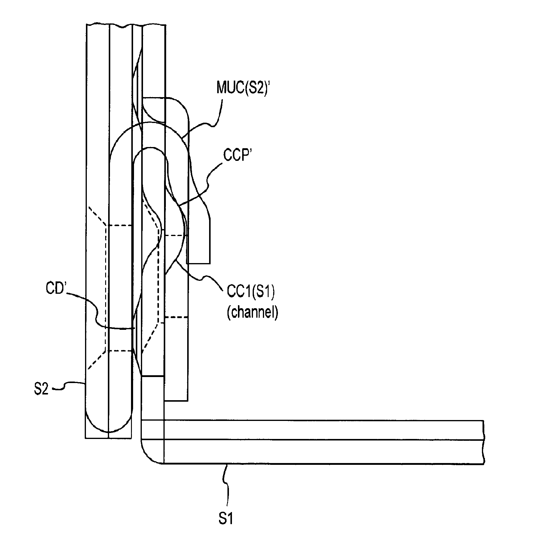
[0177]FIG. 20 illustrates the two-sheet electronics enclosure from a directly cut-away side view. An important feature not so clearly discussed above is the two-dimensional “irregular sinusoidal” (TORTURED PATH) cut K at the juncture between the upper and lower sheets. The two-dimensional cuts are discussed at detail above, and the sample shown is meant to be illustrative only. Referring now to FIG. 21, the two-sheet electronics enclosure E2 is shown. Although there are many variations that can use the various two and three dimensional features of the present invention, there are certain embodiments which allow for EMI attenuation, as well as practical and robust assembly and application. The alternate two-sheet enclosure allows for a removal of the extensions (shown in FIGS. 17-20) and adds a second partial cylinder-in-cylinder electromagnetic contact “trough.” CT2. The first contact trough CT1, is formed through partial cylindrical formation A′(S2) in the top sheet S2 which is for...
PUM
 Abstract
Description
Claims
Application Information


