Supercharge Your Innovation With Domain-Expert AI Agents!

Method for manufacturing an integrated MEMS device

a manufacturing method and integrated technology, applied in the direction of fluid speed measurement, instruments, coatings, etc., can solve the problems of reducing device performance, reducing structural reliability, degrading surface roughness and surface topography,

Active Publication Date: 2016-06-07
ASIA PACIFIC MICROSYST
View PDF13 Cites 1 Cited by
  • Summary
  • Abstract
  • Description
  • Claims
  • Application Information

AI Technical Summary

Benefits of technology

The method enables the creation of MEMS devices with enhanced planarity, hidden structural elements, and improved piezoresistive sensing capabilities, overcoming the limitations of previous technologies by maintaining the integrity of the circuit wafer and allowing for the use of high piezoresistive materials, thus improving device performance and reliability.

Problems solved by technology

This would better the device performance, but also make the manufacturing process more challenging.
The recess 13 rises from a process of manufacturing the anchor structure 12 and it would prevent the light passing therethrough from being reflected effectively, thereby reducing device performance.
However, this limitation would degrade structural reliability, surface roughness and surface topography hence total quality of the finished optical array-type device 10.

Method used


Image

  • Method for manufacturing an integrated MEMS device
  • Method for manufacturing an integrated MEMS device
  • Method for manufacturing an integrated MEMS device

Examples


Embodiment Construction

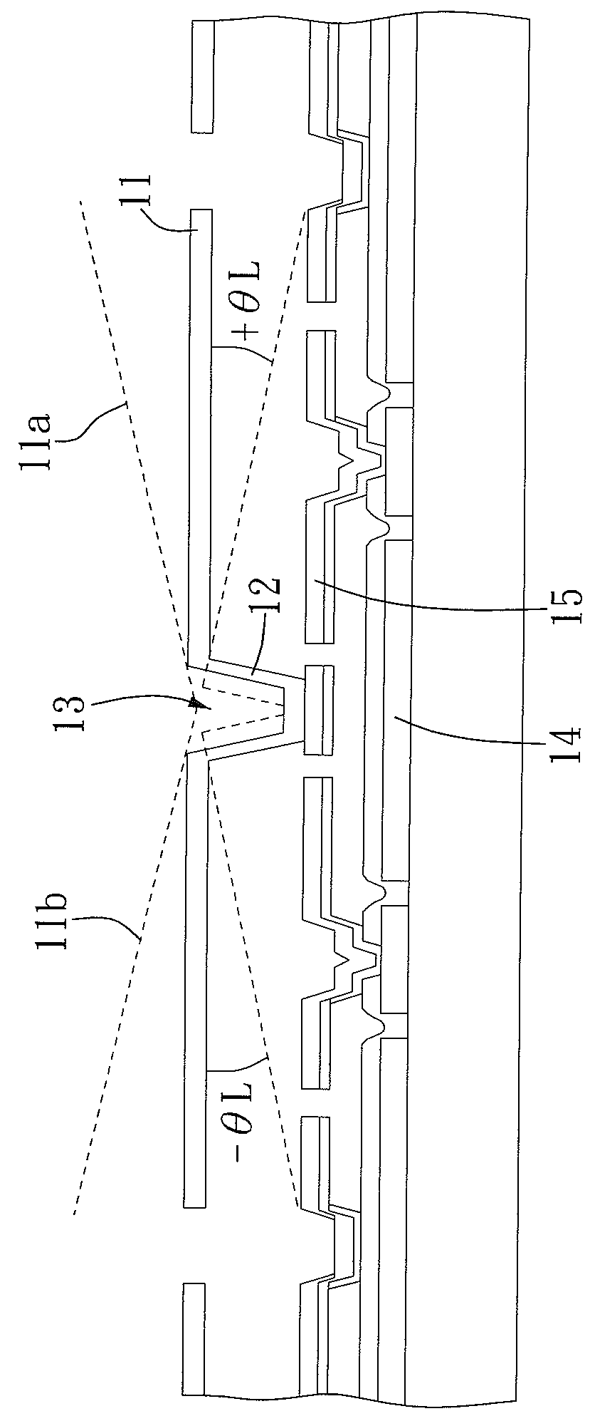
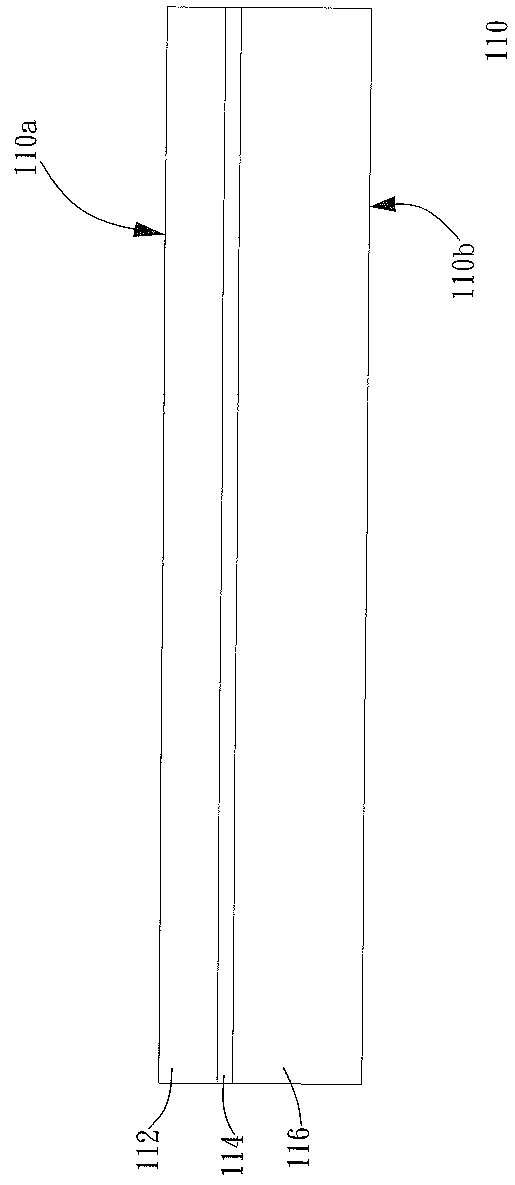
[0018]Please refer to FIGS. 2A-2J which show an embodiment of a method for manufacturing the integrated MEMS device according to one embodiment of the present invention. First, provide a device wafer 110 as shown in FIG. 2A. The device wafer 110 comprises a first surface 110a and a second surface 110b. The second surface 110b is on the opposite side of the device wafer 110 with respect to the first surface 110a. In this embodiment, the device wafer 110 is a silicon-on-insulator (SOI) structure. The device wafer 110 comprises a silicon device layer 112, an insulating layer 114 and a silicon substrate 116, wherein the first surface 110a is on the silicon device layer 112 and the second surface 110b is on the silicon substrate 116.

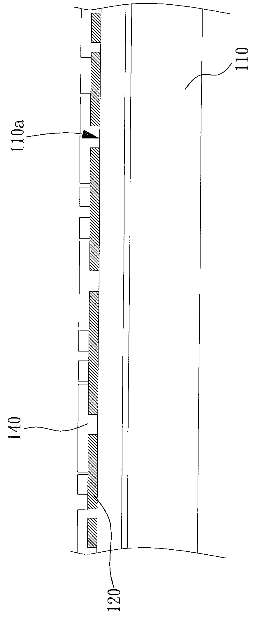
[0019]Next, as shown in FIG. 2B, a first sacrificial layer 120 and a first structural layer 140 are sequentially formed on the first surface 110a on the device wafer 110, wherein the first structural layer 140 partially covers the first sacrificial layer 120....


PUM

PropertyMeasurementUnit
temperatureaaaaaaaaaa
thicknessaaaaaaaaaa
conductiveaaaaaaaaaa

Abstract

An integrated MEMS device and its manufacturing method are provided. In the manufacturing method, the sacrificial layer is used to integrate the MEMS wafer and the circuit wafer. The advantage of the present invention comprises preventing films on the circuit wafer from being damaged during process. By the manufacturing method, a mechanically and thermally stable structure material, for example: monocrystalline silicon and polysilicon, can be used. The integrated MEMS device manufactured can also possess the merit of planar top-surface topography with high fill factor. The manufacturing method is especially suitable for manufacturing MEMS array device.

Description

FIELD OF THE INVENTION[0001]The present invention relates to an integrated MEMS device and a manufacturing method for manufacturing the same, especially a method for manufacturing an integrated MEMS device in which a MEMS wafer and a circuit wafer are bonded together first and then a sacrificial layer is removed.BACKGROUND OF THE INVENTION[0002]Techniques for integrating MEMS devices and circuit chips are important especially for the application of MEMS array-type devices. Through these techniques it is possible to integrate MEMS units of the MEMS array-type devices such as capacitive micromachined ultrasonic transducer (CMUT) and reflective micromirror array and circuit chips, thereby achieving the most effective electrical connections and control. For example, the optical array-type devices commonly adopted for many fields comprise a plurality of reflective micromirrors. These reflective micromirrors may rotate about a fixed axis to guide light toward an emitting direction. Please...

Claims


Application Information

Patent Timeline
Patent Type & Authority Patents(United States)
IPC IPC(8): H01L21/4763B81B7/00B81C1/00
CPCB81C1/00238B81B7/0058B81C1/00825B81C2201/053B81C2201/056B81C2203/0785B81C1/00817B81B7/0038B81B2201/032
Inventor HSIEH, JERWEI
Owner ASIA PACIFIC MICROSYST
Features
  • R&D
  • Intellectual Property
  • Life Sciences
  • Materials
  • Tech Scout
  • Unparalleled Data Quality
  • Higher Quality Content
  • 60% Fewer Hallucinations
Learn More