

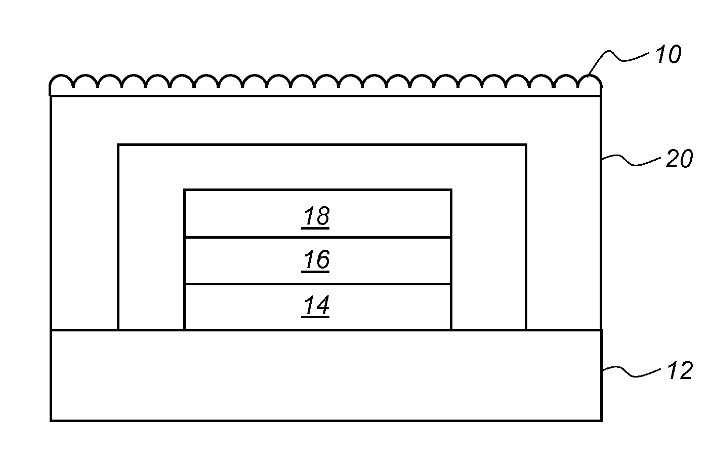
Light emitting device with microlens array
a light-emitting device and micro-lens technology, which is applied in the field of light-emitting devices having micro-lens arrays, can solve the problems of limiting the efficiency of oled devices, inefficiency in extracting photons generated by, and the fact that most of the photons generated by the recombination process are actually trapped in devices
- Summary
- Abstract
- Description
- Claims
- Application Information
AI Technical Summary
Benefits of technology
Problems solved by technology
Method used
Image

Examples
example 1
[0047]This example illustrates a method of preparation of a microlens array employed in accordance with an embodiment of the invention.
[0048]A solution containing 23.8 wt % polycarbonate (Bayer DPI 1265; surface energy 46 dynes / cm and aqueous contact angle of 70°) and 0.1% FC4-31 fluorocarbon surfactant (based on the weight of polycarbonate) in dichloromethane (specific gravity 1.33, boiling point 40 C at normal atmospheric pressure, water solubility of 1.3 g / 100 mL at 20 C and latent heat of evaporation of 406 kJ / kg) was applied on the surface of a sheet of polyethyleneterephthalate (PET) at a coverage of 452 cm3 / m2. The wet coating was then immediately inserted into a closed chamber where the temperature and humidity were controlled at 22 C and 85% RH and kept there for 5 minutes. After evaporation of the organic solvent, the sheet was kept in the chamber for an additional 5 minutes and the chamber was purged with nitrogen gas to remove residual water. The resulting dried polymer ...
example 2
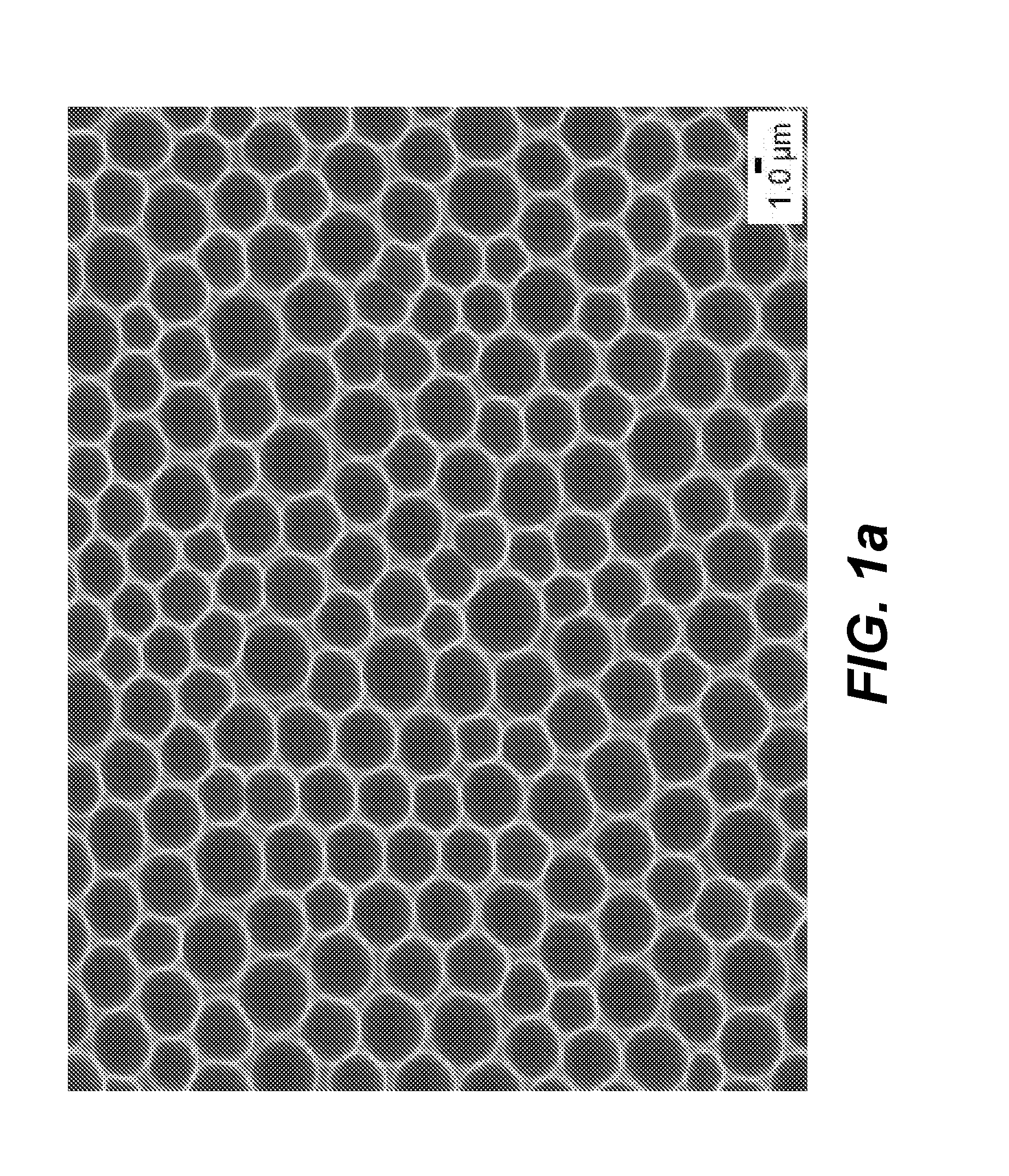
[0050]A micro-voided polymer film was prepared in the same manner as described in example 1 except that the solution that was cast on the sheet of PET did not contain any fluorocarbon surfactant FC431. As illustrated in FIG. 2, it was found that a film with a closely packed population of micro-voids was not obtained in this case and the fill factor was only about 30%. It is clear that use of the fluorocarbon surfactant in accordance with the method of the present invention enables formation of a micro-array with high fill factor and hemispherical shaped micro-lenses suitable for obtaining enhanced light output in OLED devices.
example 3
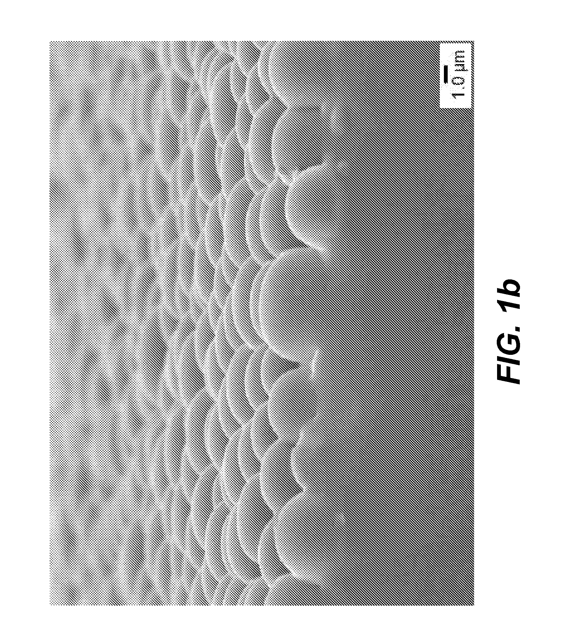
[0051]A solution containing 39.7 wt % polycarbonate (Bayer DPI 1265) and 1.0% FC431 (based on the weight of polycarbonate) in dichloromethane was applied to the surface of PET at the same coverage as in example 1, and a first structured film with surface cavities was prepared in the same manner as before. Examination of the film by optical microscopy revealed that the higher level of surfactant resulted in relatively shallower cavities, with an estimated average cavity depth to diameter ratio of less than 0.3.
[0052]Sylgard 184 elastomer was combined with curing agent and applied over the first structured film in the same manner as described in example 1. The cured elastomer film was then released from the mold to create a micro-lens array as illustrated in FIG. 3, with an estimated average lens height to diameter ratio of less than 0.3. Comparing optical micrographs of this micro-lens array with the micro-lens array resulting from the process of example 1, it is clear that the micro...
PUM
| Property | Measurement | Unit |
|---|---|---|
| diameter | aaaaa | aaaaa |
| mean diameter | aaaaa | aaaaa |
| mean diameter | aaaaa | aaaaa |
Abstract
Description
Claims
Application Information