Active pixel sensor for digital imaging

a technology of active pixel and digital imaging, which is applied in the field of digital imaging systems, can solve the problems of noise and area, and double sampling, and reducing the effect of vt non-uniformities and any dc components including low frequency flicker nois

Inactive Publication Date: 2004-07-15
NATHAN AROKIA +1
View PDF11 Cites 46 Cited by
  • Summary
  • Abstract
  • Description
  • Claims
  • Application Information

AI Technical Summary

Problems solved by technology

Hence, using a single APS cell connected directly to a charge amplifier can cause the amplifier to saturate at high VG bias values limiting the achievable gm.
The VECI circuit is highly dependent on the matching accuracy of resistors R1 and R2 and the increased number of components can cause both noise and area to increase.
In fact, double sampling greatly reduces the effect of VT non-uniformities as well as any DC components including low frequency flicker noise.
However, the penalty paid for double sampling comes in the form of extra noise.
The thermal noise components from the AMP and READ TFTs, the reset noise and the amplifier noise are all increased.
In addition, since double sampling is used, this reset noise is increased to N.sub.reset.sup.2=2kT / C.sub.eff.
Again, the presence of double sampling causes this noise variance to double.
All calculations for an a-Si TFT APS follow from CMOS APS noise theory in [16] but with characteristic a-Si TFT parameters for large area fluoroscopy, the most challenging medical imaging application.
It is notable also that the major noise contribution comes from reset noise.
The use of double sampling increases reset, thermal d charge amplifier noise but performs a low frequency filtering effect on flicker and DC noise (including any threshold voltage variations).

Method used


Image

  • Active pixel sensor for digital imaging
  • Active pixel sensor for digital imaging
  • Active pixel sensor for digital imaging

Examples


Embodiment Construction

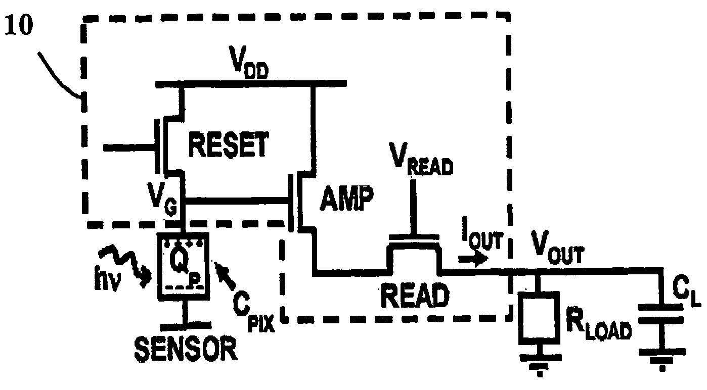
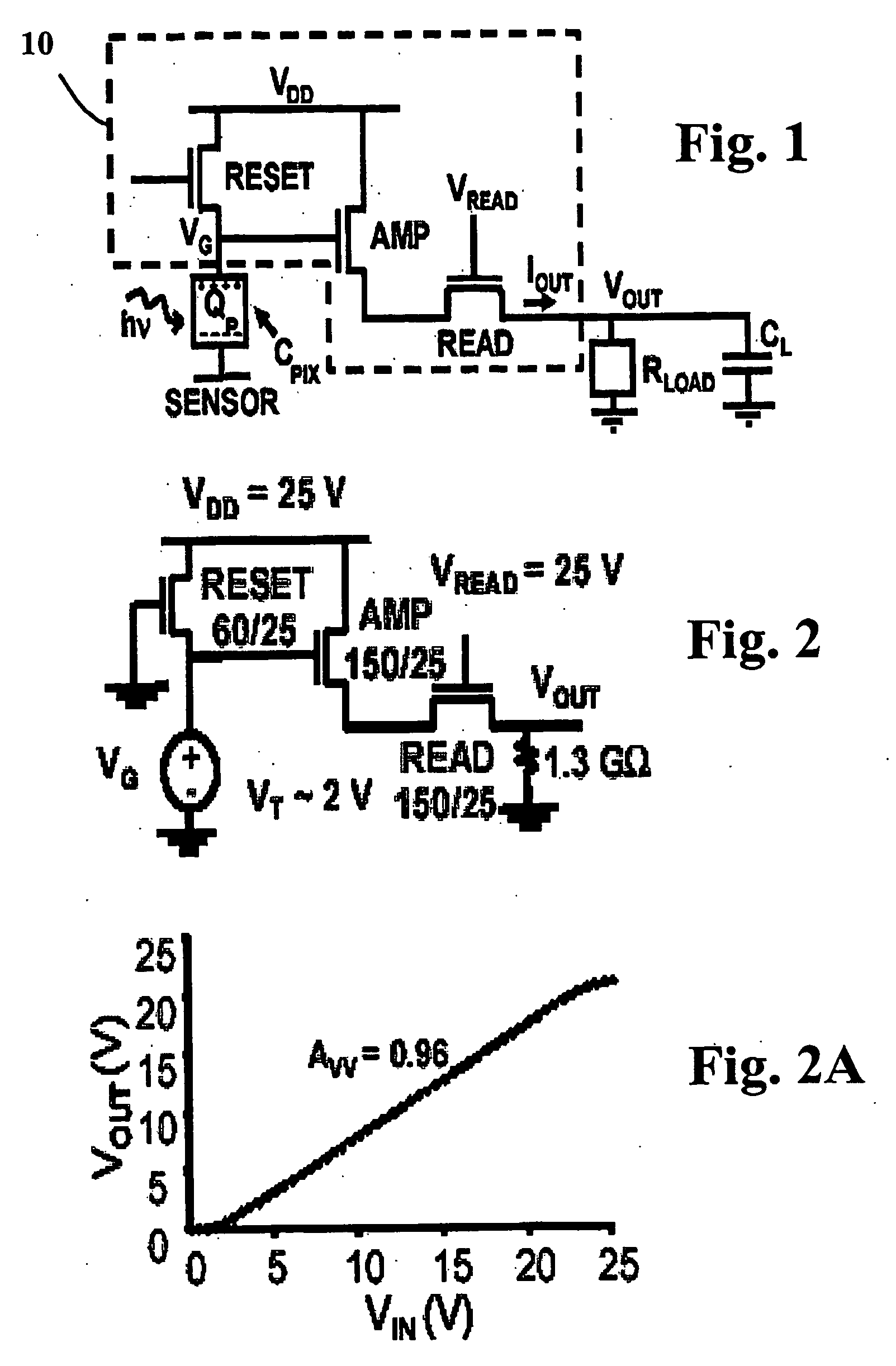
[0025] Unlike a conventional PPS, which has only one TFT switch, there are three TFTs in the APS pixel. This could undermine fill factor if conventional methods of placing the sensor and TFTs are used. Therefore, in an effort to optimize fill factor, the TFTs are assumed to be embedded under the sensor to provide high fill factor imaging systems, which follows from the continuous layer sensor architecture concept suggested previously.

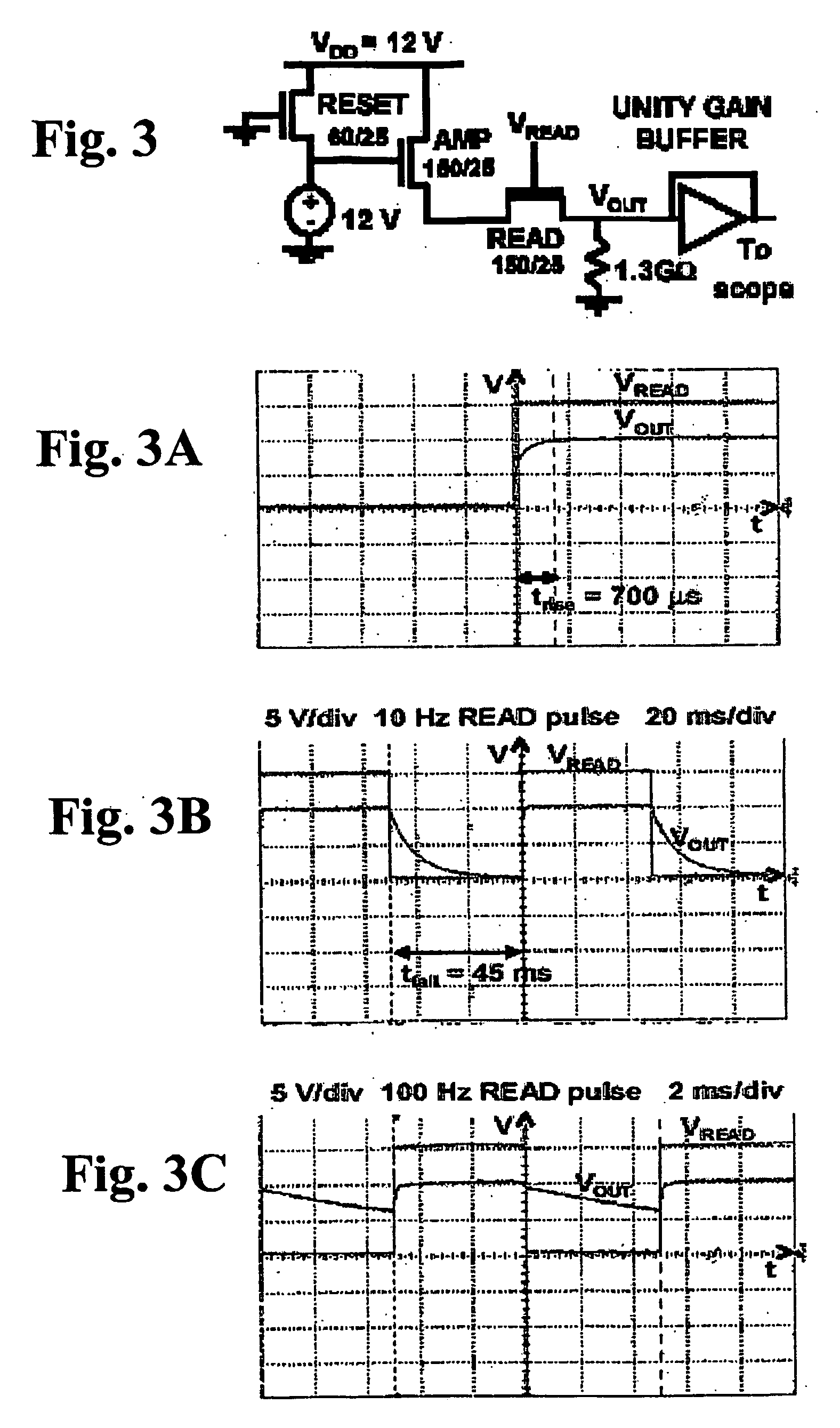
[0026] Central to the V-APS is a source follower circuit, which produces an output current that is converted to a voltage by a resistive load. The V-APS circuit is popular in CMOS imaging and is illustrated in FIG. 1. The V-APS operates in three modes: (1) Reset: The RESET TFT is switched ON and the pixel capacitance, C.sub.PIX charges up to Q.sub.p through this TFT's ON resistance, R.sub.ON.sub..sub.--.sub.RESET. (2) Integration: After reset, the RESET TFT is switched OFF for an integration period, T.sub.INT. During T.sub.INT, the x-ray input signal, h...


PUM


Abstract

An active pixel sensor for digital imaging comprises a detector, a readout circuit, and a resistive load. The detector is integrated with the readout circuit and the readout circuit has a plurality of amorphous silicon based thin-film transistors (TFTs). The readout circuit is embedded under the detector to provide a high fill factor. A signal charge is accumulated on a pixel capacitance during an integration mode and is transferred to an external electronics for data acquisition via the readout circuit during a readout mode. An output current from the readout circuit is converted to a voltage through the resistive load. The resistive load may be a thin-film transistor operated in a saturation regime and having a width larger than a length in size. The active pixel sensor amplifies an on-pixel sensor input signal to improve a noise immunity of sensitive sensor input signals to external noise sources and its linearity together with a fast pixel readout time.

Description

[0001] 1. Field of the Invention[0002] The present invention relates to digital imaging system, and more particularly to an active pixel sensor (APS) for digital imaging.[0003] 2. Description of the Prior Art[0004] Amorphous silicon (a-Si) active matrix flat-panel imagers (AMFPIs) have gained considerable significance in digital imaging, and more recently in diagnostic medical imaging applications, in view of their large area readout capability. The pixel, forming the fundamental unit of the active matrix, consists of a detector and readout circuit to efficiently transfer the collected electrons to external electronics for data acquisition. The pixel architecture most commonly used is the passive pixel sensor (PPS) where a detector (e.g. amorphous selenium (a-Se) based photoconductor or CsI phosphor coupled to an a-Si:H p-i-n photodiode) is integrated with a readout circuit comprising a thin-film transistor (TFT) switch. Signal charge is accumulated on the pixel capacitance (which i...

Claims


Application Information

Patent Timeline
Patent Type & Authority Applications(United States)
IPC IPC(8): H01L27/146H01L31/00
CPCH01L27/14658
Inventor NATHAN, AROKIAKARIM, KARIM S.
Owner NATHAN AROKIA
Why Eureka
Try Eureka