
Decoding method, decoding circuit, memory storage device and controlling circuit unit

a decoding circuit and memory storage device technology, applied in the field of decoding methods, can solve the problems of limited correction capability and increase decoding latency, and achieve the effect of reducing decoding latency

Active Publication Date: 2016-06-07
PHISON ELECTRONICS
View PDF3 Cites 1 Cited by
  • Summary
  • Abstract
  • Description
  • Claims
  • Application Information

AI Technical Summary

Benefits of technology

The invention is about a method, device, and circuit for quickly decoding low density parity codes. This is done by iteratively checking and outputting the index of errors in the code. This method reduces decoding latency, making it faster and more efficient.

Problems solved by technology

The error correcting codes in conventional art usually adopts an algebraic decoding algorithm such as BCH code, in which a correcting capability is limited.
In some implementations, inputting and outputting the entire codeword may increase a decoding latency to expand demands for bandwidth of a buffer memory.

Method used


Image

  • Decoding method, decoding circuit, memory storage device and controlling circuit unit
  • Decoding method, decoding circuit, memory storage device and controlling circuit unit
  • Decoding method, decoding circuit, memory storage device and controlling circuit unit

Examples


first exemplary embodiment

[0037]Generally, a memory storage device (also known as a memory storage system) includes a rewritable non-volatile memory module and a controller (also known as a control circuit). The memory storage device is usually configured together with a host system so that the host system may write data to or read data from the memory storage device.

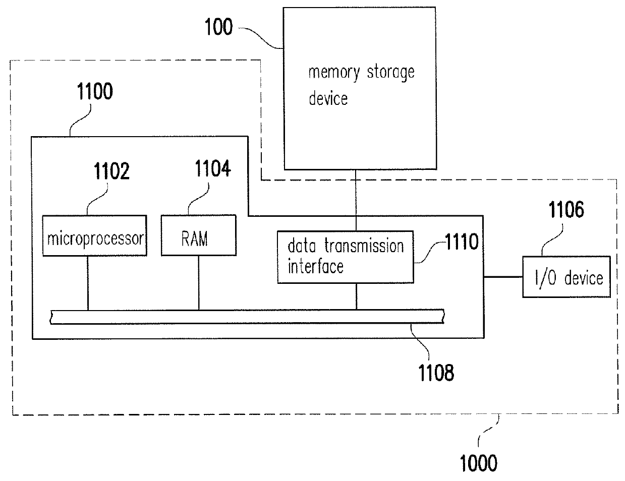
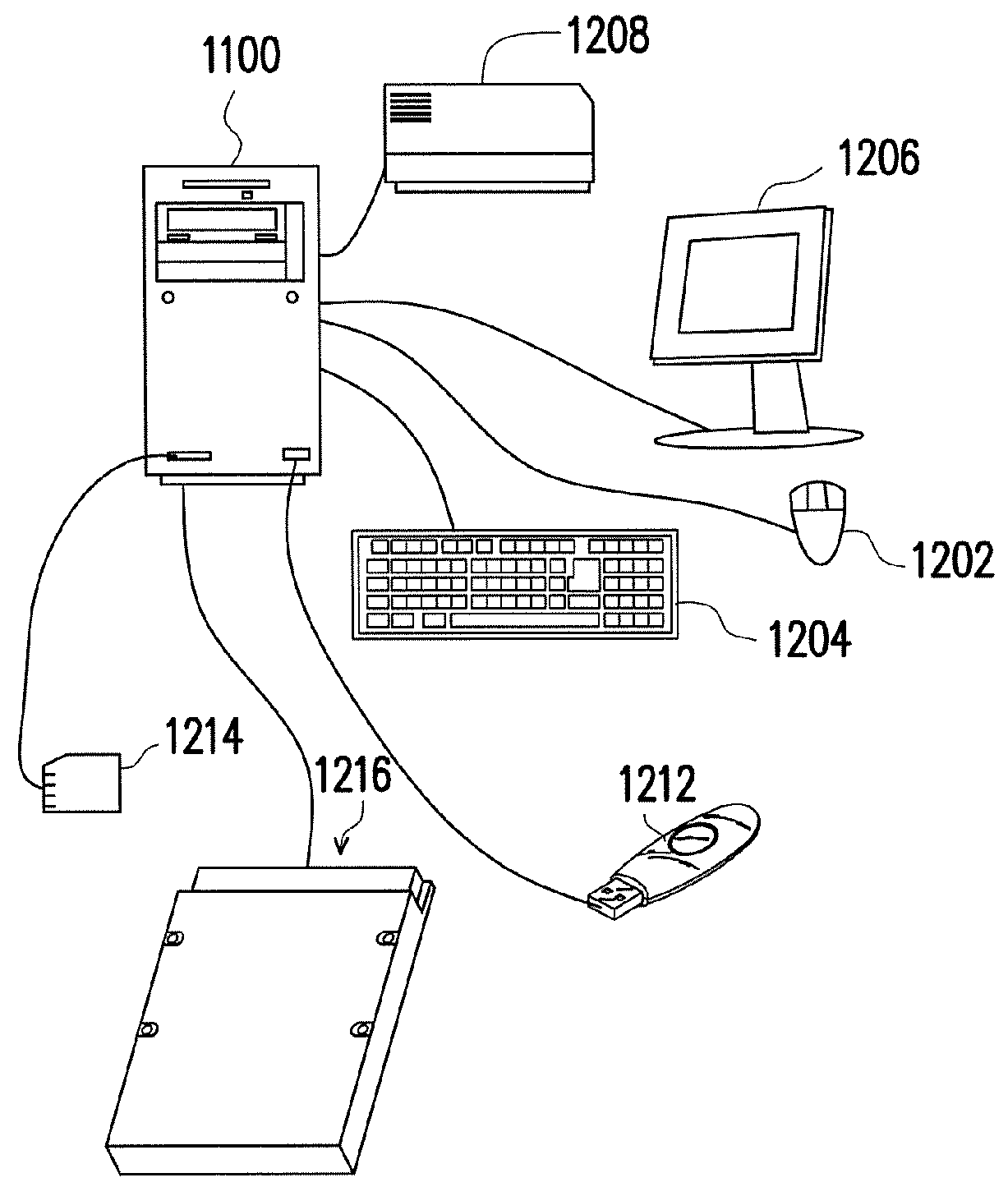
[0038]FIG. 1 illustrates a host system and a memory storage device according to an exemplary embodiment. FIG. 2 is a schematic diagram illustrating a computer, an input / output device and a memory storage device according to an exemplary embodiment.

[0039]Referring to FIG. 1, a host system 1000 includes a computer 1100 and an input / output (I / O) device 1106. The computer 1100 includes a microprocessor 1102, a random access memory (RAM) 1104, a system bus 1108, and a data transmission interface 1110. For example, the I / O device 1106 includes a mouse 1202, a keyboard 1204, a display 1206 and a printer 1208 as shown in FIG. 2. It should be understood ...

second exemplary embodiment

[0076]In second exemplary embodiment, when the memory management circuit 202 reads the data bits from rewritable non-volatile memory module 106, a plurality of read voltages are used to obtain a plurality of verification bits form each of the first memory cells, in which one read voltage is corresponding to one of the verification bits. The verification bits may be used to decide the data bit, or may be used to obtain a channel reliability message. The iterative decoding preformed in case each of the memory cells includes multiple verification bits is referred to as a soft bit mode decoding.

[0077]FIG. 13 illustrates a schematic diagram of reading a verification bit according to an exemplary embodiment. Referring to FIG. 13, it is assumed that the memory cell in a storage status 1510 stores the bit “1”, and the memory cell in a storage status 1520 stores the bit “0”. The storage status 1510 may be partially overlapped with the storage status 1520, namely, under some specific read vol...

third exemplary embodiment

[0094]Hereinafter, only differences between third embodiment and second embodiment are described below. In third exemplary embodiment, the memory management circuit 202 may obtain the verification bit of the memory cell by only using one read voltage. The iterative decoding preformed in this case is referred to as a hard bit mode decoding. Furthermore, in third exemplary embodiment, the number of the channel reliability message is one. More specifically, after reading a verification bit of each of the first memory cells according to a read voltage, the memory management circuit 202 may obtain a log likelihood ratio of each of the first memory cells according to the corresponding verification bit. The memory management circuit 202 may also calculate an average value of the log likelihood ratios of the first memory cells to serve as the channel reliability message, namely, all of the data bits are corresponding to the same channel reliability message.

[0095]In a first iteration of thir...


PUM


Abstract

A decoding method, a memory storage device, a memory controlling circuit unit and a decoding circuit for low density parity code (LDPC) are provided. The decoding method includes: reading a data bit of each memory cell; performing a parity check procedure on the data bits to generate a plurality of checks; in an iterative decoding of LDPC, obtaining a reliability message of each data bit according to the checks and deciding an index of an error bit from the data bits according to the reliability messages; determining whether the index of the error bit and the checks comply with a parity criteria; and if the index of the error bit and the checks comply with the parity criteria, stopping the iterative decoding and outputting the index of the error bit. Accordingly, a decoding latency is decreased.

Description

CROSS-REFERENCE TO RELATED APPLICATION[0001]This application claims the priority benefit of Taiwan application serial no. 102138141, filed on Oct. 22, 2013. The entirety of the above-mentioned patent application is hereby incorporated by reference herein and made a part of this specification.BACKGROUND[0002]1. Technical Field[0003]The invention relates to a decoding method, and more particularly, to a decoding method, a memory storage device, a memory controlling circuit unit and a decoding circuit for a low density parity code.[0004]2. Description of Related Art[0005]The markets of digital cameras, cellular phones, and MP3 players have expanded rapidly in recent years, resulting in escalated demand for storage media by consumers. The characteristics of data non-volatility, low power consumption, and compact size make the rewritable non-volatile memory module (e.g., flash memory) ideal for being built in the portable multi-media devices as cited above.[0006]Generally, some error cor...

Claims


Application Information

Patent Timeline
Patent Type & Authority Patents(United States)
IPC IPC(8): G11C29/00G06F11/10H03M13/11
CPCH03M13/1105G06F11/1012H03M13/1108H03M13/1111H03M13/1117
Inventor TSENG, CHIEN-FU
Owner PHISON ELECTRONICS
Learn More