Supercharge Your Innovation With Domain-Expert AI Agents!

Etching method for forming grooves in Si-substrate and fin field-effect transistor

a technology of field-effect transistors and etching methods, which is applied in the direction of transistors, semiconductor devices, electrical apparatus, etc., can solve the problems of insufficient si-substrate groove formation and inability to retain the specific contour of grooves, so as to improve the electrical performance of devices

Active Publication Date: 2016-06-21
UNITED MICROELECTRONICS CORP
View PDF18 Cites 1 Cited by
  • Summary
  • Abstract
  • Description
  • Claims
  • Application Information

AI Technical Summary

Benefits of technology

[0005]Hence, according to the invention, an etching method for forming grooves in Si-substrate and a fin field-effect transistor (FinFET) as manufactured thereby are provided, so as to meet the distinct electrical requirements for various types of fin field-effect transistor (FinFET) devices, and improve the electrical performance of devices.

Problems solved by technology

Under the circumstances, it will become insufficient to form grooves in the Si-substrate by simply utilizing a single etching process.
However, once several etching processes have been carried out, it will become impossible to retain the specific contours of grooves, since the pre-formed grooves will suffer from the problem of over-etching, resulted from the corrosion by subsequent etching processes.

Method used


Image

  • Etching method for forming grooves in Si-substrate and fin field-effect transistor
  • Etching method for forming grooves in Si-substrate and fin field-effect transistor
  • Etching method for forming grooves in Si-substrate and fin field-effect transistor

Examples


Embodiment Construction

[0018]The embodiments will now be described more specifically with reference to the following embodiments. It is to be noted that the following descriptions of preferred embodiments are presented herein for purpose of illustration and description only. It is not intended to be exhaustive or to be limited to the precise form disclosed.

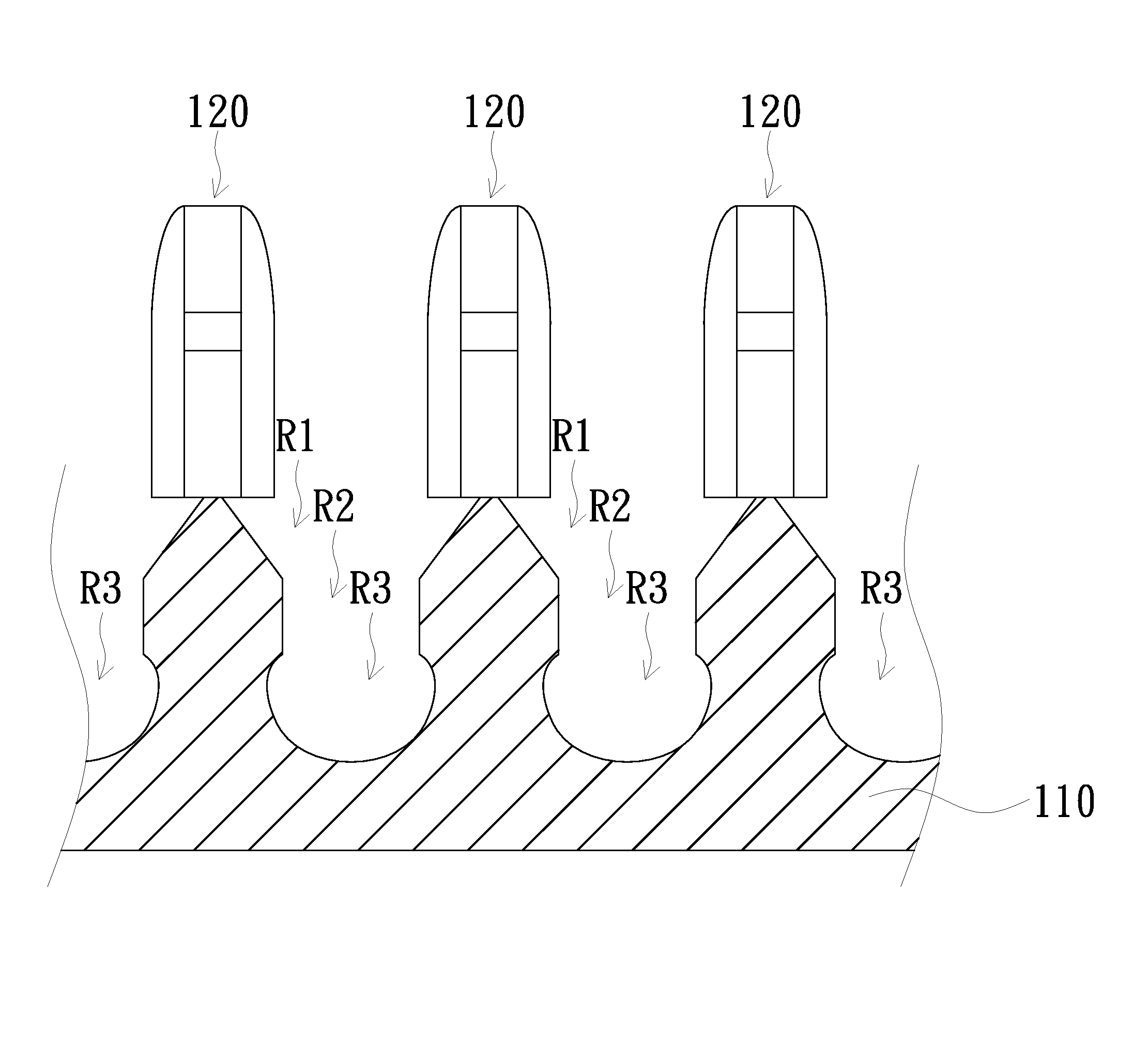
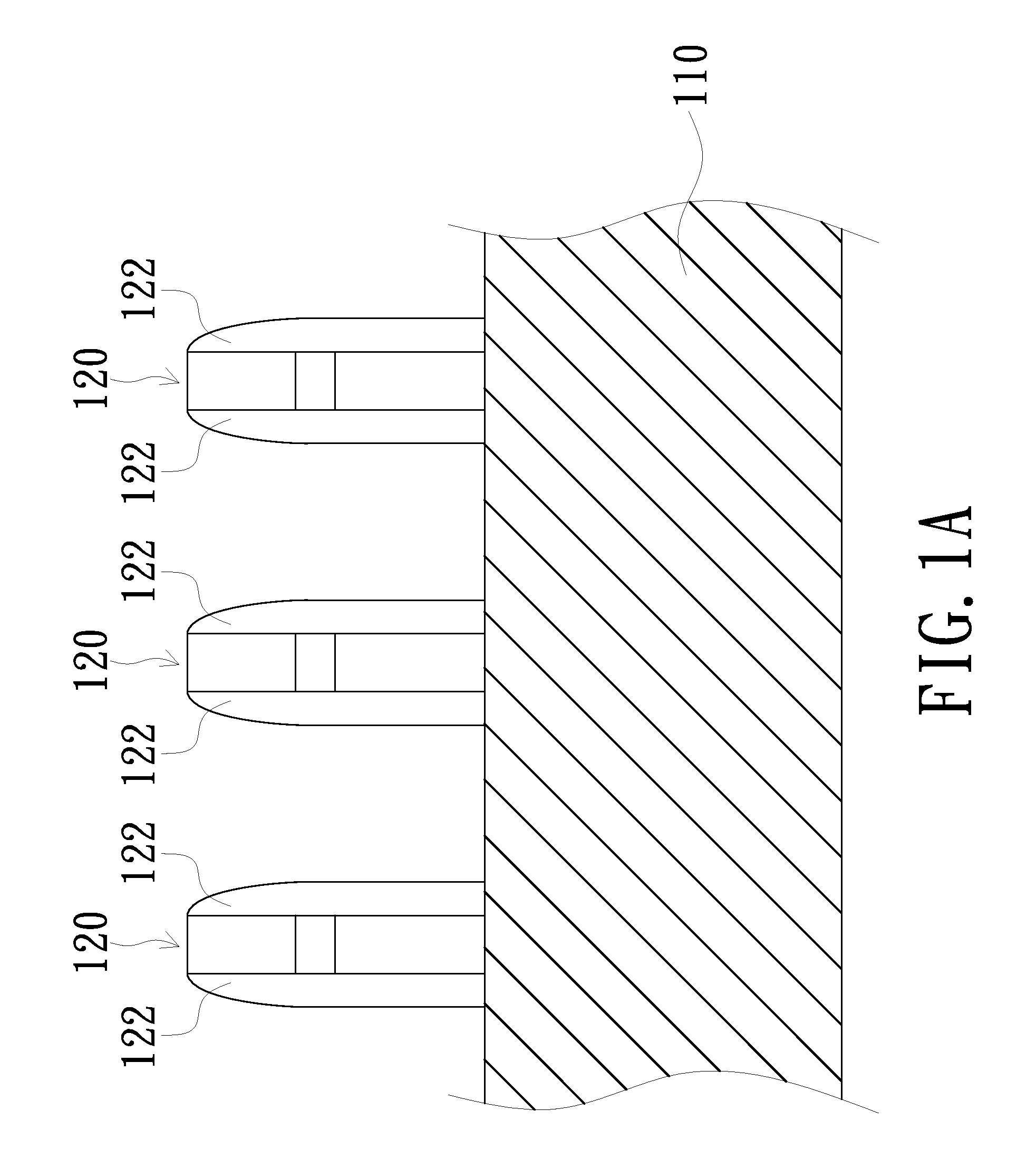
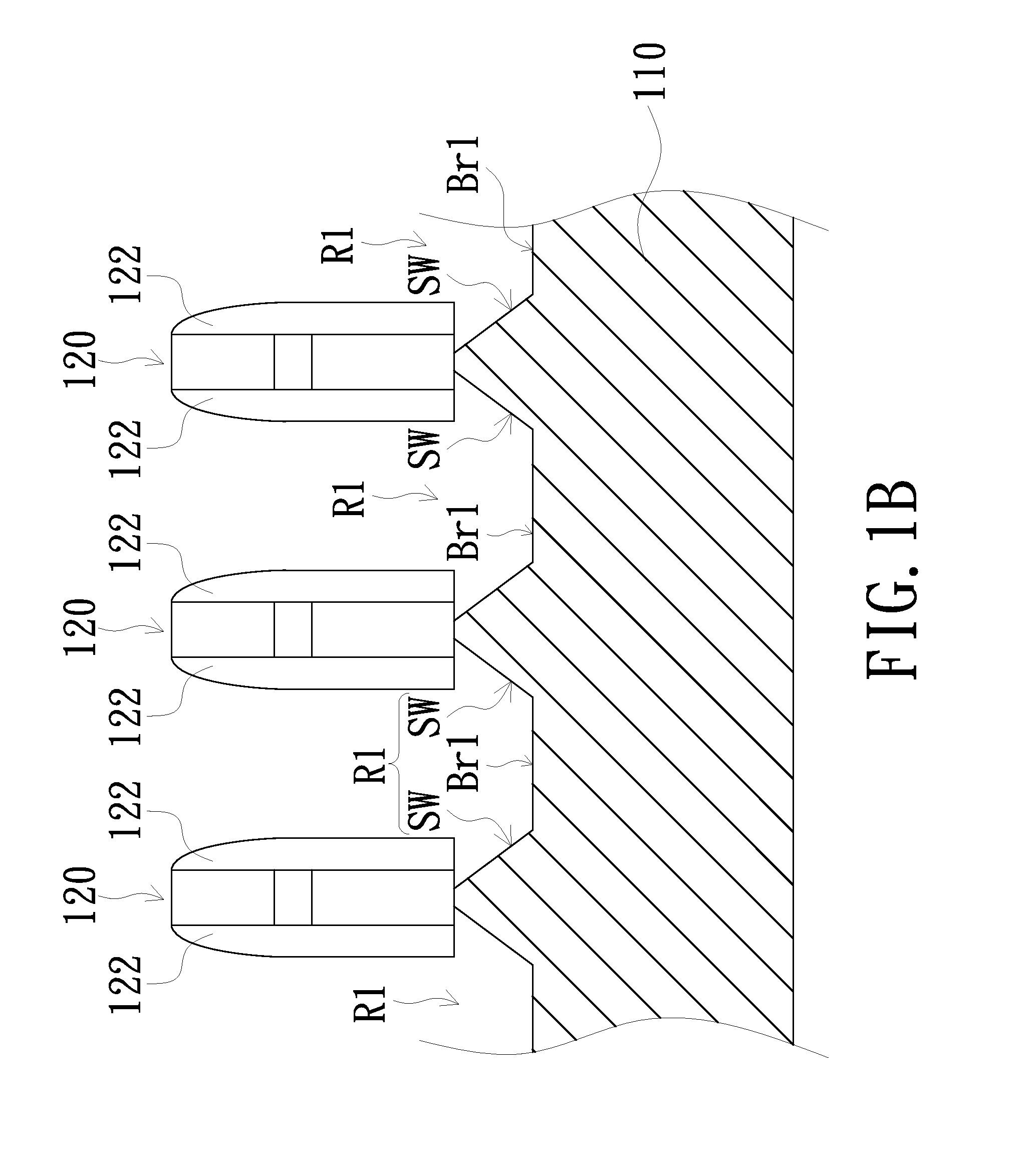
[0019]FIGS. 1A-1F are cross-sectional views illustrating an etching method adapted for forming grooves in Si-substrate according to one embodiment of the invention. Firstly, by referring to FIGS. 1A-1B as a whole, according to the one embodiment of the invention, the etching method adapted for forming grooves in Si-substrate includes providing a silicon substrate 110, wherein the silicon substrate 110 has at least two gate structures 120, and respective sidewalls of the gate structures 120 are encircled by a gate spacer structure 122; performing a first etching process on the silicon substrate 110 for forming a first groove R1, wherein the first groove ...


PUM


Abstract

An etching method adapted to forming grooves in Si-substrate and FinFET transistor manufactured thereof are provided. The etching method includes providing a silicon substrate, at least two gate structures formed on the silicon substrate and at least two gate spacer structures disposed on the silicon substrate; performing a first etching process on the silicon substrate to form a first groove, which has a base and two inclined sidewalls, ascending to respective bottoms of the gate structures, and are interconnected with the base, respectively; and performing a second etching process on the silicon substrate at the base of the first groove, so as to form a second groove in an inverted -symbol shape, wherein the two inclined sidewalls of the first groove are interconnected with the second groove respectively, and the first etching process is substantially different from the second etching process.

Description

FIELD OF THE INVENTION[0001]The invention relates to an etching method and semiconductor device structure, and more particularly to an etching method adapted for forming grooves in Si-substrate and a fin field-effect transistor (FinFET) manufactured thereby.BACKGROUND OF THE INVENTION[0002]When employing semiconductor processes for manufacturing a fin field-effect transistor (FinFET), it is always essential to grow a superior silicon germanium epitaxial material layer in a silicon substrate. Besides, prior to the growth of the silicon germanium epitaxial layer, it is necessary to form grooves in the silicon substrate, and then grow the silicon germanium epitaxial layer in the grooves in the Si-substrate.[0003]However, since there are distinct electrical requirements for various types of transistor devices, it thus becomes necessary to grow silicon germanium epitaxial material layers in various shapes and depths. Under the circumstances, it will become insufficient to form grooves in...

Claims


Application Information

Patent Timeline
Patent Type & Authority Patents(United States)
IPC IPC(8): H01L21/336H01L21/311H01L27/088H01L21/8234H01L21/02H01L21/3065H01L21/306H01L29/66H01L29/161H01L29/165H01L29/78
CPCH01L29/165H01L29/161H01L27/0886H01L21/823431H01L21/823418H01L21/31138H01L21/31116H01L21/3065H01L21/30604H01L21/02238H01L21/02164H01L29/7848H01L21/02118H01L29/7851H01L29/66795H01L29/66636H01L21/823412H01L21/823425H01L21/3083
Inventor LI, JHEN-CYUANLU, SHUI-YENLU, MAN-LINGTUNG, YU-CHENGCHANG, CHUNG-FU
Owner UNITED MICROELECTRONICS CORP
Features
  • R&D
  • Intellectual Property
  • Life Sciences
  • Materials
  • Tech Scout
  • Unparalleled Data Quality
  • Higher Quality Content
  • 60% Fewer Hallucinations
Learn More