Network-on-chip architecture for multi-processor SoC designs

a technology of network-on-chip architecture and soc design, applied in the field of network-on-chip architecture design, can solve the problem that the bus-based topology cannot meet the very demanding needs of today's on-chip communication

Active Publication Date: 2016-09-06
ADVANCED MICRO DEVICES INC
View PDF4 Cites 20 Cited by
  • Summary
  • Abstract
  • Description
  • Claims
  • Application Information

AI Technical Summary

Problems solved by technology

Bus-based topologies clearly cannot satisfy the very demanding needs of today's on-chip communication because of the lack of scalability; only one component pair can communicate at a time, and the load capacitance of the entire bus has to be driven during each data transfer.

Method used


Image

  • Network-on-chip architecture for multi-processor SoC designs
  • Network-on-chip architecture for multi-processor SoC designs
  • Network-on-chip architecture for multi-processor SoC designs

Examples


Embodiment Construction

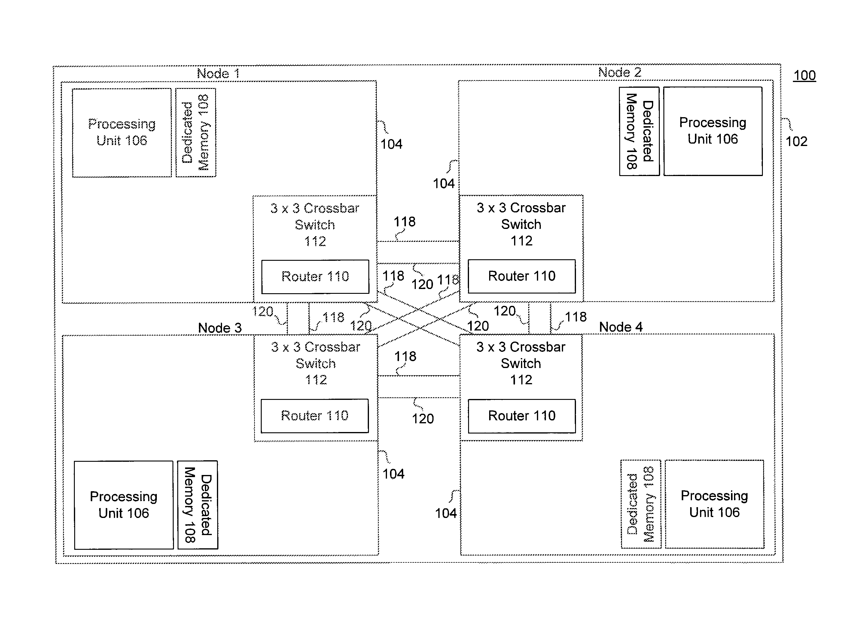
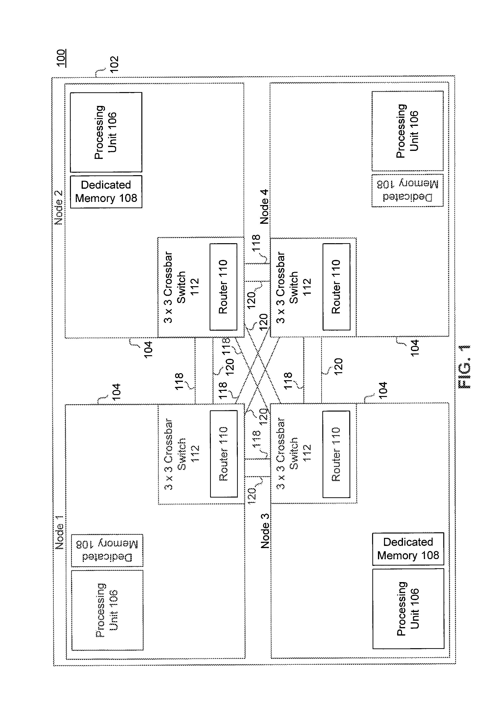
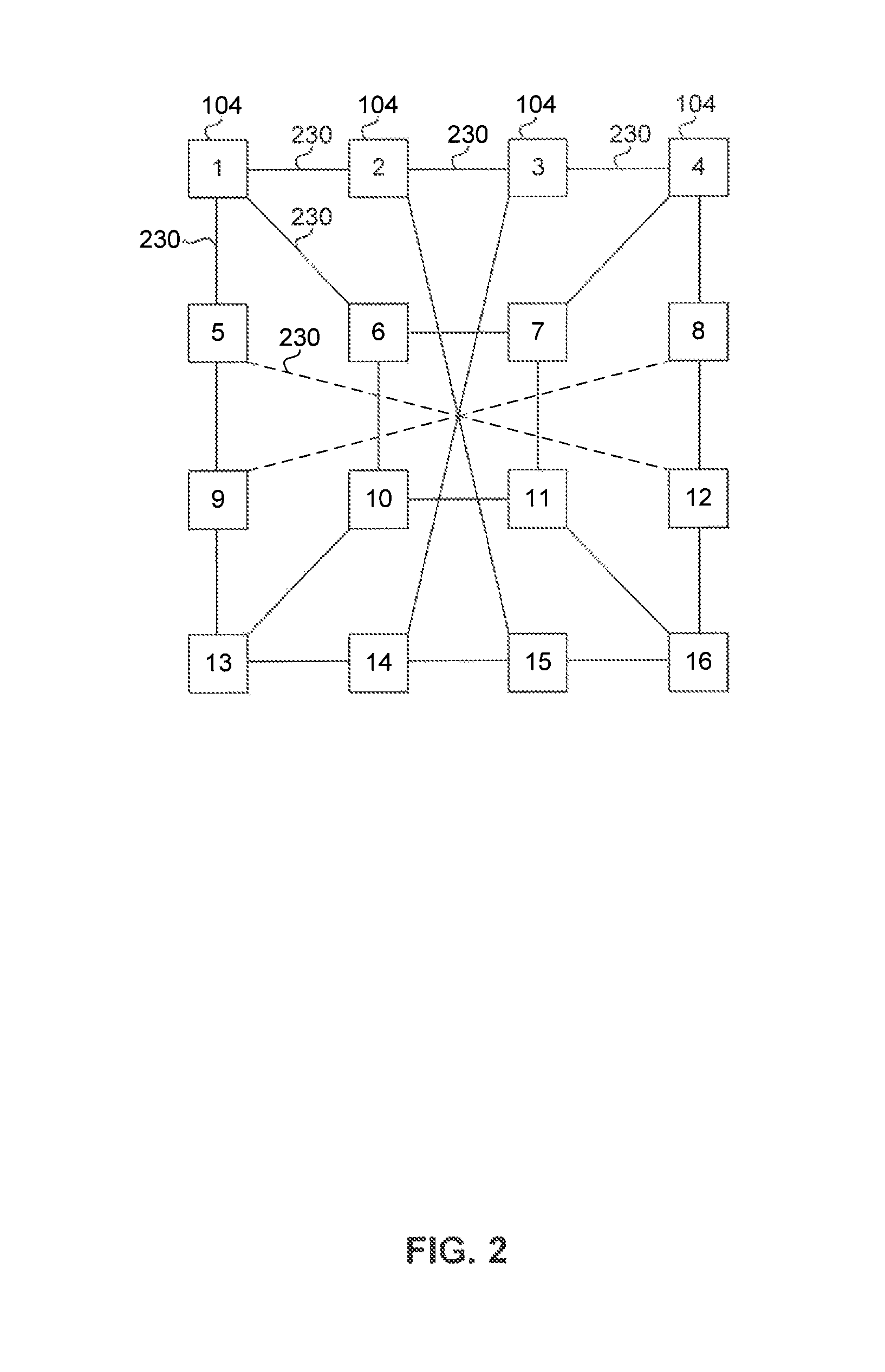
[0007]A system and method embodying some embodiments for communicating between nodes in a network-on-chip are provided. The system comprises a microprocessing chip and a plurality of connection paths. The microprocessing chip comprises sixteen processing nodes disposed on the chip. The plurality of connection paths are configured such that each is at most three hops away from any other node. Each node also has connection paths to at most three other nodes.

[0008]Further features and advantages of the embodiments, as well as the structure and operation of various embodiments, are described in detail below with reference to the accompanying drawings. It is noted that the embodiments are not limited to the specific embodiments described herein. Such embodiments are presented herein for illustrative purposes only. Additional embodiments will be apparent to persons skilled in the relevant art(s) based on the teachings contained herein.

BRIEF DESCRIPTION OF THE DRAWINGS / FIGURES

[0009]The acc...


PUM


Abstract

A system and method embodying some aspects for communicating between nodes in a network-on-chip are provided. The system comprises a microprocessing chip and a plurality of connection paths. The microprocessing chip comprises sixteen processing nodes disposed on the chip. The plurality of connection paths are configured such that each is at most three hops away from any other node. Each node also has connection paths to at most three other nodes.

Description

BACKGROUND[0001]1. Field[0002]The embodiments are generally directed to Network-on-Chip architecture designs. More particularly, the embodiments are directed to efficient communication between nodes in a Network-on-Chip architecture.[0003]2. Background Art[0004]As technology scales down, an increasing number of designs are getting integrated on the same silicon die, causing demand for on-chip communication architecture. Many system-on-a-chip (SoC) designs use commercially available bus-based topologies, such as VME, AMBA, and CoreConnect, for on-chip communication because of their simple architectures and low area costs. Bus-based topologies clearly cannot satisfy the very demanding needs of today's on-chip communication because of the lack of scalability; only one component pair can communicate at a time, and the load capacitance of the entire bus has to be driven during each data transfer.[0005]Switch-based network design was proposed as an alternative to bus-based topologies. A s...

Claims


Application Information

Patent Timeline
Patent Type & Authority Patents(United States)
IPC IPC(8): G06F13/40G06F15/173
CPCG06F13/4022G06F15/17368
Inventor KOMMANABOYINA, SUDARSHANAM
Owner ADVANCED MICRO DEVICES INC
Why Eureka
Try Eureka