Method of manufacturing a photovoltaic device

a photovoltaic device and manufacturing method technology, applied in the field of photovoltaic devices, can solve the problems of poor interface between the semiconductor layer and the back contact layer, which may have an undesirable effect on the photovoltaic device, and negatively affect the grain boundary and/or lattice of the crystals forming the semiconductor layer, so as to improve the performance of the photovoltaic device

Active Publication Date: 2016-09-20
FIRST SOLAR INC
View PDF13 Cites 8 Cited by
  • Summary
  • Abstract
  • Description
  • Claims
  • Application Information

AI Technical Summary

Benefits of technology

[0006]Concordant and congruous with the instant disclosure, a more effective method to remove surface contaminants from an absorber layer of a photovoltaic device prior to depositing or forming a back contact layer to improve a performance of the photovoltaic device has surprisingly been discovered.

Problems solved by technology

Contaminants formed on the semiconductor layer may affect an interface between the semiconductor layer and the back contact layer.
A poor interface between the semiconductor layer and the back contact layer may have an undesirable effect on the photovoltaic device, and specifically on VOC and ROC.
Known methods of removing contaminants from the surface of the semiconductor layer may negatively affect a grain boundary and / or lattice of the crystals forming the semiconductor layer.

Method used


Image

  • Method of manufacturing a photovoltaic device
  • Method of manufacturing a photovoltaic device

Examples


Embodiment Construction

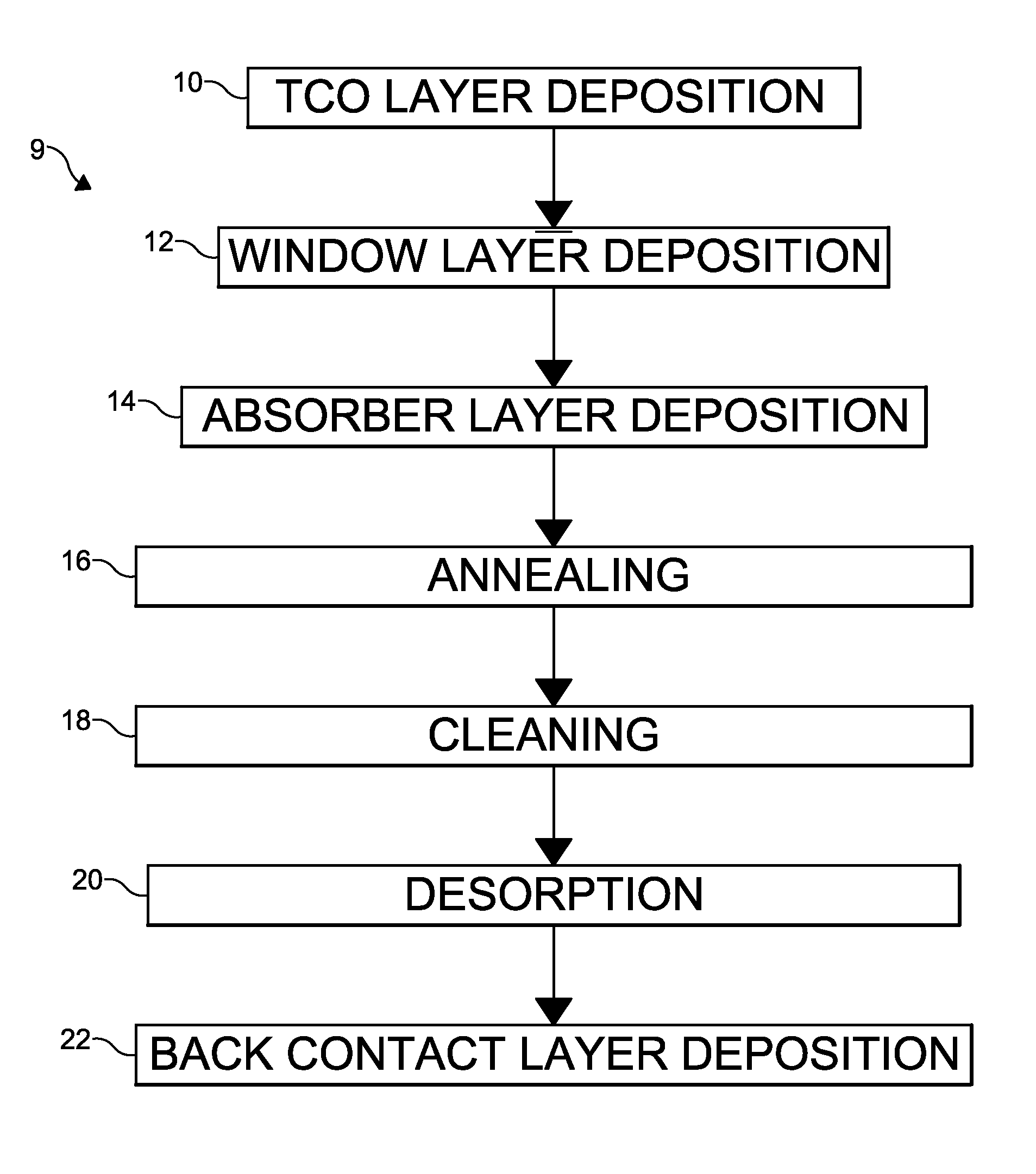
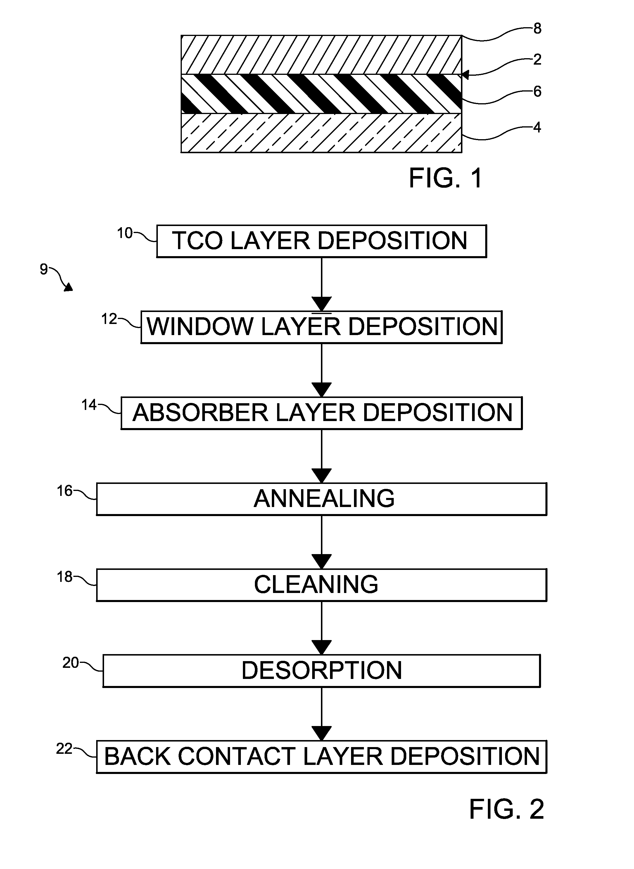
[0013]The following description is merely exemplary in nature and is not intended to limit the present disclosure, application, or uses. It should also be understood that throughout the drawings, corresponding reference numerals indicate like or corresponding parts and features. In respect of the methods disclosed, the order of the steps presented is exemplary in nature, and thus, is not necessary or critical unless recited otherwise.

[0014]As shown in FIG. 1 the present disclosure includes a photovoltaic device 2. The photovoltaic device 2 has multiple layers including a glass substrate (or superstrate) 4, a semiconductor layer 6 (also referred to as an absorber layer or a semiconductor absorber layer), and a back contact layer 8. For purposes of simplicity in illustrating the invention, only the substrate 4, the semiconductor layer 6, and the back contact layer 8 are shown in the drawings. However, one of ordinary skill in the art should understand that one or more additional layer...


PUM


Abstract

A method to improve CdTe-based photovoltaic device efficiency is disclosed, the method including steps for removing surface contaminants from a semiconductor absorber layer prior to the deposition or formation of a back contact layer on the semiconductor absorber layer, the surface contaminants removed using at least one of a dry etching process and a wet etching process.

Description

CROSS-REFERENCE TO RELATED APPLICATION[0001]This is application claims the benefit of priority of U.S. Provisional Patent Application Ser. No. 61 / 791,442 filed on Mar. 15, 2013 hereby incorporated herein by reference in its entirety.FIELD OF THE INVENTION[0002]The present disclosure relates to a photovoltaic device, and more particularly to a method of preparing a surface of a photovoltaic device prior to deposition of an additional layer to improve an interface therebetween.BACKGROUND OF THE INVENTION[0003]Photovoltaic modules, devices, or cells, can include multiple layers (or coatings) created on a substrate (or superstrate). For example, a photovoltaic device can include a barrier layer, a transparent conductive oxide layer, a buffer layer, and a semiconductor layer formed in a stack on a substrate. Each layer may in turn include more than one layer or film. For example, a semiconductor window layer and a semiconductor absorber layer together can be considered a semiconductor la...

Claims


Application Information

Patent Timeline
Patent Type & Authority Patents(United States)
IPC IPC(8): H01L21/00H01L31/0224H01L31/0392H01L31/073
CPCH01L31/022425H01L31/03925H01L31/073Y02E10/543H01L31/1828H01L31/186Y02P70/50
Inventor CHRISTENSEN, SCOTTMROZEK, PAWELXIONG, GANGYU, SAN
Owner FIRST SOLAR INC
Why Eureka
Try Eureka