Antimony-base compound thin film solar cell and manufacturing method thereof

A technology of solar cells and oxide thin films, applied in circuits, electrical components, photovoltaic power generation, etc., can solve the problems of toxic production process, low element content and high price, and achieve the effect of excellent photovoltaic performance and abundant resources.

Inactive Publication Date: 2014-11-12
HUAZHONG UNIV OF SCI & TECH
View PDF7 Cites 14 Cited by
  • Summary
  • Abstract
  • Description
  • Claims
  • Application Information

AI Technical Summary

Problems solved by technology

[0003] The invention provides an antimony-based compound thin-film solar cell and a preparation method thereof, which solve the problem that the elements contained in the required materials in th

Method used


Image

  • Antimony-base compound thin film solar cell and manufacturing method thereof
  • Antimony-base compound thin film solar cell and manufacturing method thereof
  • Antimony-base compound thin film solar cell and manufacturing method thereof

Examples


Embodiment 1

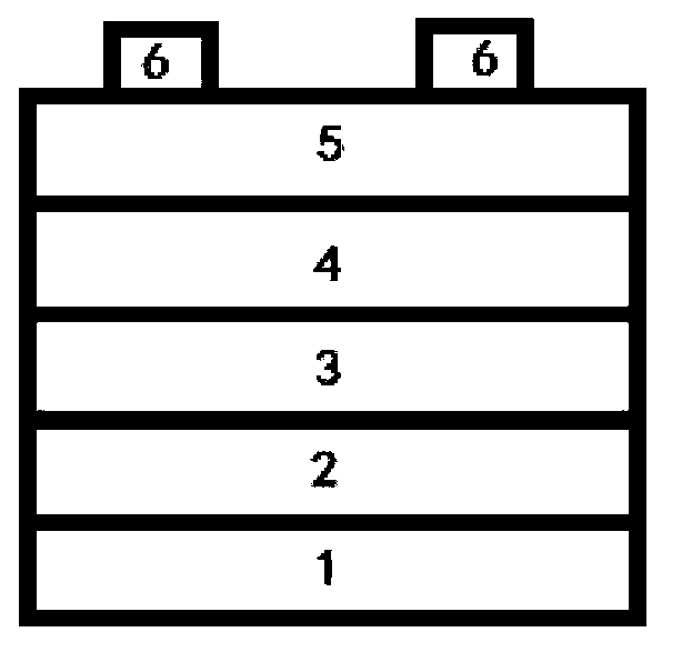
[0047] Embodiment 1, the preparation method of antimony-based compound thin-film solar cells, including the steps of depositing a back electrode layer, depositing a P-type absorber layer, depositing an N-type buffer layer, depositing an oxide film window layer, and depositing a metal gate electrode:

[0048] 1. The step of depositing the back electrode layer: depositing the back electrode layer 2 on the surface of the substrate 1 by magnetron sputtering;

[0049] The substrate is glass with a thickness of 1.8cm;

[0050] The back electrode layer is Mo with a thickness of 800nm;

[0051] 2. The step of depositing a P-type absorbing layer: using a solution coating method to deposit a P-type absorbing layer 3 on the back electrode layer 2;

[0052] The P-type absorption layer material is CuSbS 2 , with a thickness of 1.5 μm;

[0053] Cu:Sb:S was dissolved in hydrazine at a ratio of 1:1:7 by solution coating method to form CuSbS 2 precursor, CuSbS was coated with a film coater...

Embodiment 2

[0063] Embodiment 2, the preparation method of antimony-based compound thin-film solar cells, including the steps of depositing a back electrode layer, depositing a P-type absorber layer, depositing an N-type buffer layer, depositing an oxide film window layer, and depositing a metal gate electrode:

[0064] 1. The step of depositing the back electrode layer: depositing the back electrode layer 2 on the surface of the substrate 1 by magnetron sputtering;

[0065] The substrate is glass with a thickness of 3cm;

[0066] The back electrode layer is SnO 2 : F; the thickness is 1000nm;

[0067] 2. The step of depositing a P-type absorbing layer: using a solution coating method to deposit a P-type absorbing layer 3 on the back electrode layer 2;

[0068] The P-type absorption layer material is CuSbS 2 , with a thickness of 1.5 μm; the surface morphology under the scanning electron microscope is as follows Figure 7 Shown; cyclic voltammetry curve as Figure 8 Shown; Raman spec...

Embodiment 3

[0076] Embodiment 3, the preparation method of antimony-based compound thin-film solar cells, including the steps of depositing a back electrode layer, depositing a P-type absorber layer, depositing an N-type buffer layer, depositing an oxide film window layer, and depositing a metal gate electrode:

[0077] 1. The step of depositing the back electrode layer: depositing the back electrode layer 2 on the surface of the substrate 1 by magnetron sputtering;

[0078] The substrate is polyimide with a thickness of 0.01cm;

[0079] The back electrode layer is In 2 o 3 :Sn; thickness is 100nm;

[0080] 2. The step of depositing a P-type absorbing layer: using a thermal evaporation method to deposit a P-type absorbing layer 3 on the back electrode layer 2;

[0081] The P-type absorption layer material is CuSbS 2 , with a thickness of 0.8 μm;

[0082] 3. The step of depositing an N-type buffer layer: using a chemical water bath method to deposit an N-type buffer layer 4 on the P-typ...


PUM

PropertyMeasurementUnit
Thicknessaaaaaaaaaa
Thicknessaaaaaaaaaa
Thicknessaaaaaaaaaa

Abstract

The invention discloses an antimony-base compound thin film solar cell and a manufacturing method of the antimony-base compound thin film solar cell and belongs to the manufacturing field of photoelectric material and thin film solar cells. The problems that in an existing compound thin film solar cell, needed material is little in the earth crust, high in price and toxic to the human body or complex in production technology are solved. The antimony-base compound thin film solar cell comprises a substrate, a back electrode layer, a P-type absorption layer, an N-type buffering layer, an oxide thin film window layer and metal gate electrodes in a sequential deposition mode. The P-type absorption layer is made of CuXSbybetaZ material, wherein beta is S or Se. The material of the P-type absorption layer is selected from high-abundance elements in the earth crust, wherein the material is rich in resource and environmentally friendly because no toxic components are contained, the range of the energy gap of the elements is about 0.5 ev-2.5 ev, the spectral response range is wide, the light absorption coefficient is up to 105 cm-1, and therefore the compound thin film solar battery composed of the material has excellent photovoltaic performance and is environmentally friendly, and low-cost production is expected to be achieved.

Description

technical field [0001] The invention belongs to the field of photoelectric materials and thin-film solar cell preparation, and in particular relates to an antimony-based compound thin-film solar cell and a preparation method thereof. Background technique [0002] With the development of the economy, the demand for energy has increased sharply, the depletion of non-renewable energy and the environmental pollution caused by the combustion of fossil fuels have become more prominent. Solar cells, as a clean and pollution-free new energy source, have received a lot of attention. A solar cell is a device that uses the photovoltaic effect to directly convert solar energy into electrical energy. Multi-component compound thin-film solar cells have received more attention due to their advantages such as less material consumption, low energy consumption for preparation, good low-light and high-temperature performance, light weight, flexible cells, and wide application range. The exist...

Claims


Application Information

Patent Timeline
IPC IPC(8): H01L31/072H01L31/0352H01L31/0224H01L31/032H01L31/18
CPCH01L31/032H01L31/072H01L31/18Y02E10/50Y02P70/50
Inventor 唐江韩珺杨波周英王亮刘新胜冷美英
Owner HUAZHONG UNIV OF SCI & TECH
Why Eureka
Try Eureka