Advanced process flow for quantum memory devices and josephson junctions with heterogeneous integration

a technology of quantum memory and process flow, applied in the direction of dissimilar materials junction devices, superconductor devices, instruments, etc., can solve the problems of limiting the minimum device area, final achievable circuit density, and overall circuit reliability

Active Publication Date: 2016-09-27
THE UNITED STATES OF AMERICA AS REPRESENTED BY THE SECRETARY OF THE NAVY
View PDF2 Cites 37 Cited by
  • Summary
  • Abstract
  • Description
  • Claims
  • Application Information

AI Technical Summary

Benefits of technology

[0004]Disclosed herein is a process for constructing a superconducting Josephson-based nonvolatile quantum memory device. An embodiment of the process comprises the following steps. The first step involves providing a silicon substrate. The next step provides for depositing a thermal oxide buffer layer on the substrate. The next step provides for depositing a superconductor bottom-electrode thin film on the thermal oxide buffer layer. The next step provides for depositing an oxide isolation layer by low-pressure chemical vapor deposition (LPCVD) on the superconductor bottom-electrode thin film. The next step provides for patterning an active window having dimensions smaller that 10 nanometers (nm) in the oxide isolation layer. The next step provides for depositing a bottom tunnel oxide layer on the oxide isolation layer and the active window via thermal atomic layer deposition (ALD). The next step provides for depositing a charge-trapping layer via pl...

Problems solved by technology

Unfortunately, anodization results in consumption of ˜60-80 nm of the superconductor film (e.g. Nb) and can cause degradation of the active tu...

Method used


Image

  • Advanced process flow for quantum memory devices and josephson junctions with heterogeneous integration
  • Advanced process flow for quantum memory devices and josephson junctions with heterogeneous integration
  • Advanced process flow for quantum memory devices and josephson junctions with heterogeneous integration

Examples


Embodiment Construction

[0013]The disclosed methods and systems below may be described generally, as well as in terms of specific examples and / or specific embodiments. For instances where references are made to detailed examples and / or embodiments, it should be appreciated that any of the underlying principles described are not to be limited to a single embodiment, but may be expanded for use with any of the other methods and systems described herein as will be understood by one of ordinary skill in the art unless otherwise stated specifically.

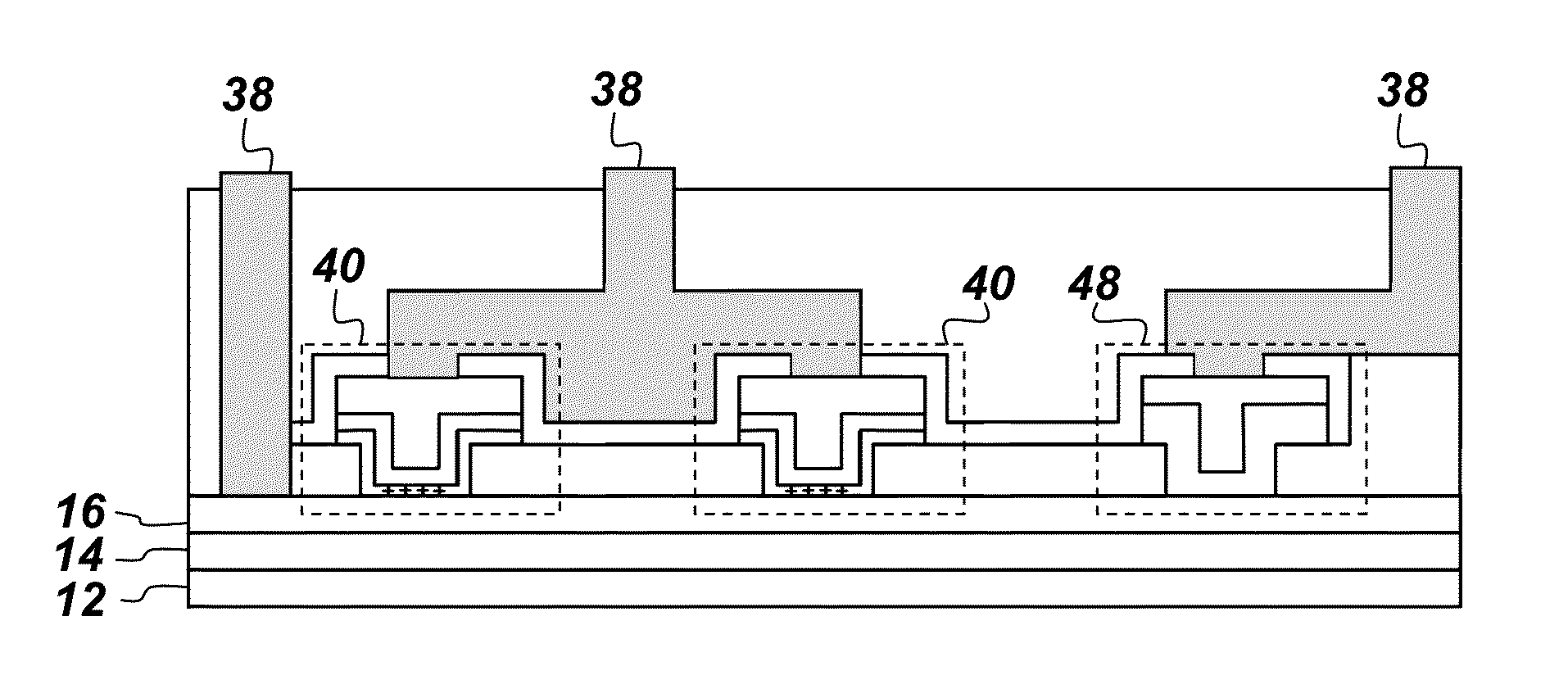
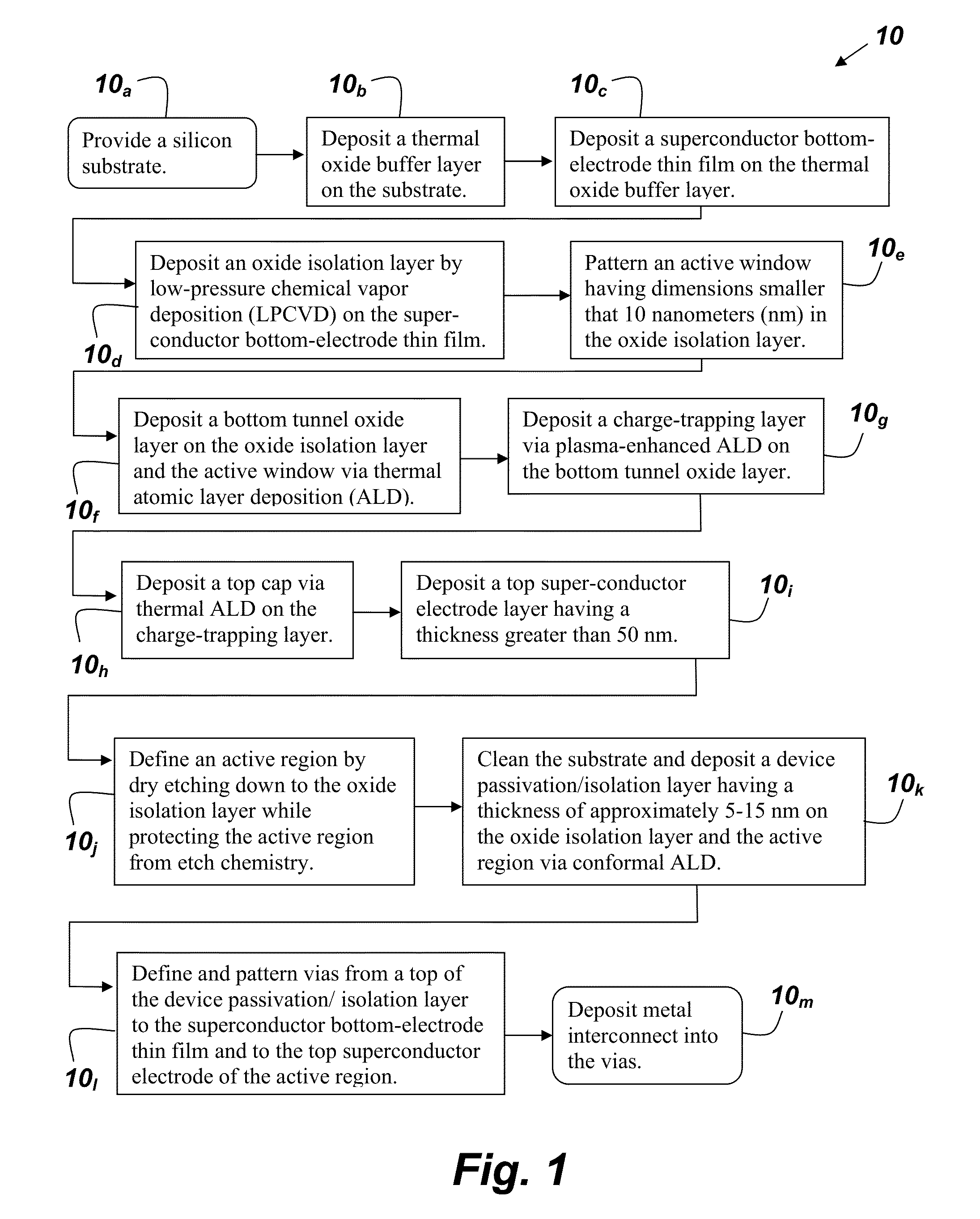
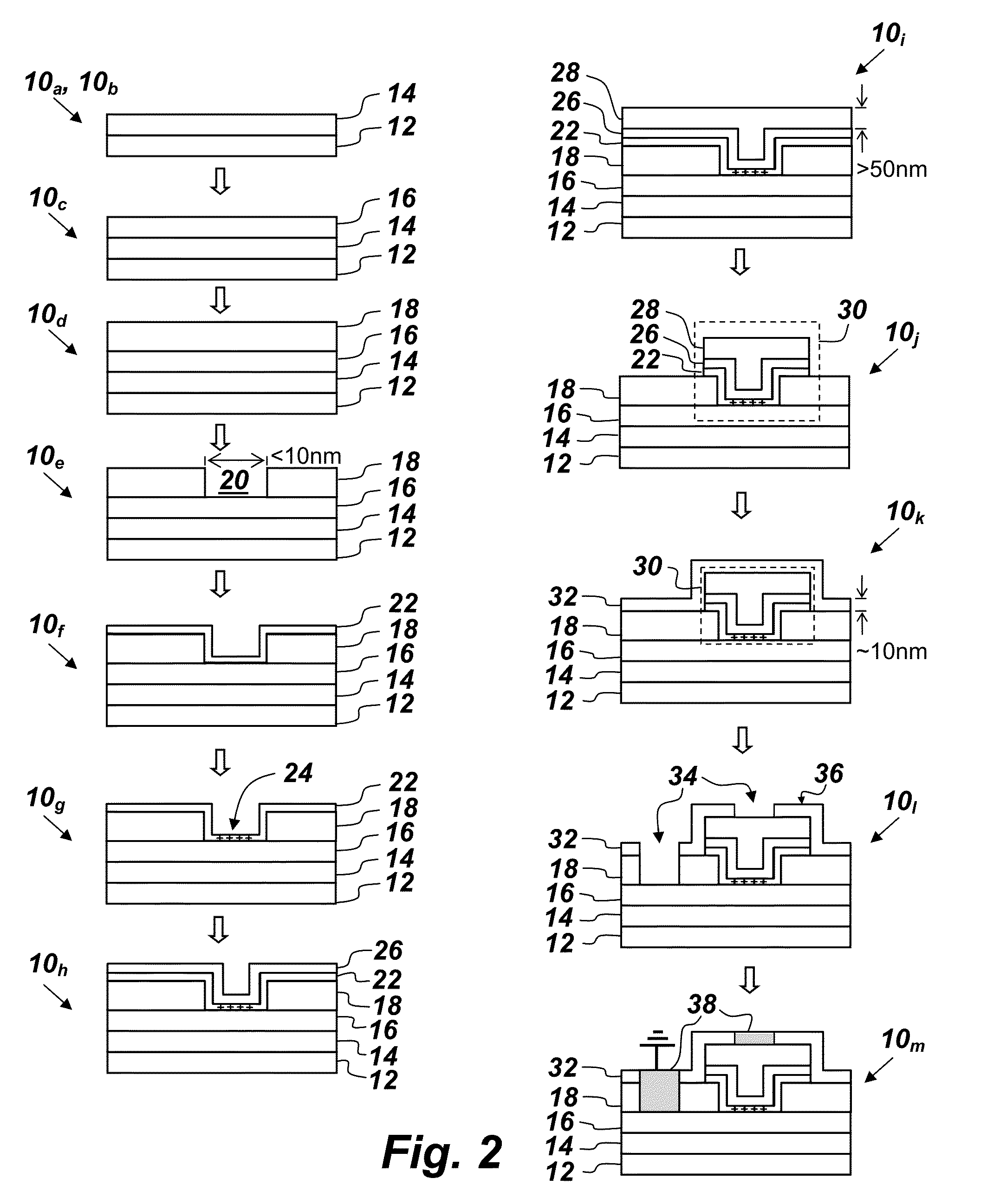
[0014]FIG. 1 is a flowchart of an embodiment of a process 10 for constructing a superconducting Josephson-based nonvolatile quantum memory device. Process 10 comprises, consists of, or consists essentially of the following steps. Step 10a involves providing a silicon substrate. Step 10b provides for depositing a thermal oxide buffer layer on the substrate. Step 10c provides for depositing a superconductor bottom-electrode thin film on the thermal oxide buffer layer. ...


PUM


Abstract

A process for constructing a superconducting Josephson-based nonvolatile quantum memory device comprising: sequentially depositing on a silicon substrate a thermal oxide buffer layer, a superconductor bottom-electrode thin film, and an oxide isolation layer; patterning an active window having dimensions smaller that 10 nanometers in the oxide isolation layer; then sequentially depositing a bottom tunnel oxide layer, a charge-trapping layer, a top cap, and a top superconductor electrode layer; defining an active region by dry etching down to the oxide isolation layer while protecting the active region from etch chemistry; depositing a device passivation layer; defining and patterning vias from a top of the device passivation layer to the superconductor bottom-electrode thin film and to the top superconductor electrode of the active region; and depositing metal interconnect into the vias.

Description

FEDERALLY-SPONSORED RESEARCH AND DEVELOPMENT[0001]The United States Government has ownership rights in this invention. Licensing and technical inquiries may be directed to the Office of Research and Technical Applications, Space and Naval Warfare Systems Center, Pacific, Code 72120, San Diego, Calif., 92152; voice (619) 553-5118; ssc_pac_t2@navy.mil. Reference Navy Case Number 102933.CROSS-REFERENCE TO RELATED APPLICATION[0002]This application is related to U.S. application Ser. No. 14 / 716,629, filed 19 May 2015, titled “Quantum Memory Device and Method” (Navy Case #102361), which application is hereby incorporated by reference herein in its entirety for its teachings. This application is also related to U.S. application Ser. No. 15 / 060,290, filed 3 Mar. 2016, titled “Reconfigurable, Tunable Quantum Qubit Circuits with Internal, Nonvolatile Memory” (Navy Case #102561), which application is hereby incorporated by reference herein in its entirety for its teachings.BACKGROUND OF THE IN...

Claims


Application Information

Patent Timeline
IPC IPC(8): H01L21/8239H01L39/22H01L27/18H01L39/24
CPCH01L39/223H01L27/18H01L39/2493G11C11/44H10N69/00H10N60/12H10N60/0912
Inventor NAYFEH, OSAMA M.DINH, SONLEESE DE ESCOBAR, ANNASIMONSEN, KENNETH
Owner THE UNITED STATES OF AMERICA AS REPRESENTED BY THE SECRETARY OF THE NAVY
Why Eureka
Try Eureka