Backside transparent substrate roughening for UV light emitting diode

a technology of backside and transparent substrate, which is applied in the direction of basic electric elements, electrical apparatus, semiconductor devices, etc., can solve the problems of reducing the efficiency of light generation in the leds, and affecting the efficiency of light extraction in the leds, so as to reduce the post growth processing steps and simplify the post growth processing

Inactive Publication Date: 2016-10-04
RAYVIO
View PDF40 Cites 18 Cited by
  • Summary
  • Abstract
  • Description
  • Claims
  • Application Information

AI Technical Summary

Benefits of technology

[0007]In the present invention, a fabrication process for epitaxy onto back-side patterned substrate, where the substrate patterns were defined prior to epitaxy and therefore simplify post growth processing. Specifically, for LED devices, said fabrication process reduces the post growth processing steps required to obtain high LEE due to strong scattering of the back-side features defined on the substrate. The features defined on the back-side patterned substrate scatters strongly with light emitted from the LED devices. Methods of obtaining such features include wet and dry etching.

Problems solved by technology

Light emitting diodes (LEDs) based on InAlGaN multiple quantum wells (MQWs) generally suffer from certain limitations in terms of energy efficiency to produce light.
One limitation is to efficiently extract light generated in the MQWs from inside the LEDs to air.
Such photons eventually are lost inside the LEDs due to intrinsic material losses and other absorption mechanisms.
Despite significant advances achieved in improving the LEE, most of the existing approaches require post epi-growth processing which can be quite complex and potentially affects the yield, reliability and cost of the LEDs.

Method used


Image

  • Backside transparent substrate roughening for UV light emitting diode
  • Backside transparent substrate roughening for UV light emitting diode
  • Backside transparent substrate roughening for UV light emitting diode

Examples


Embodiment Construction

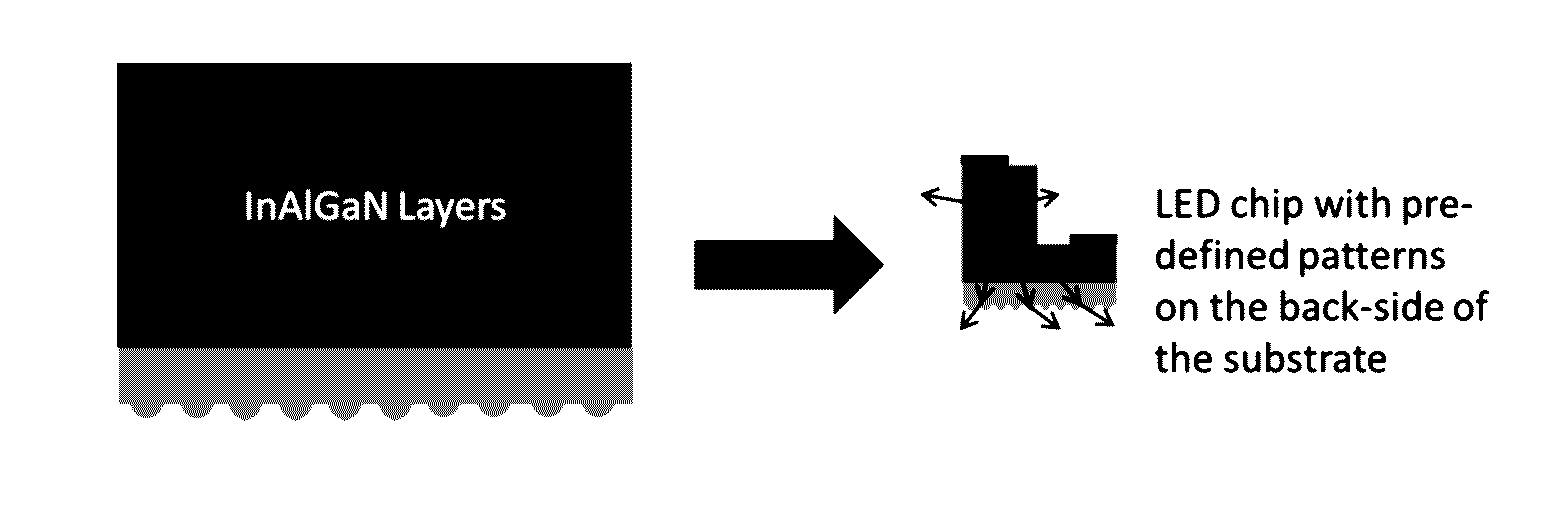
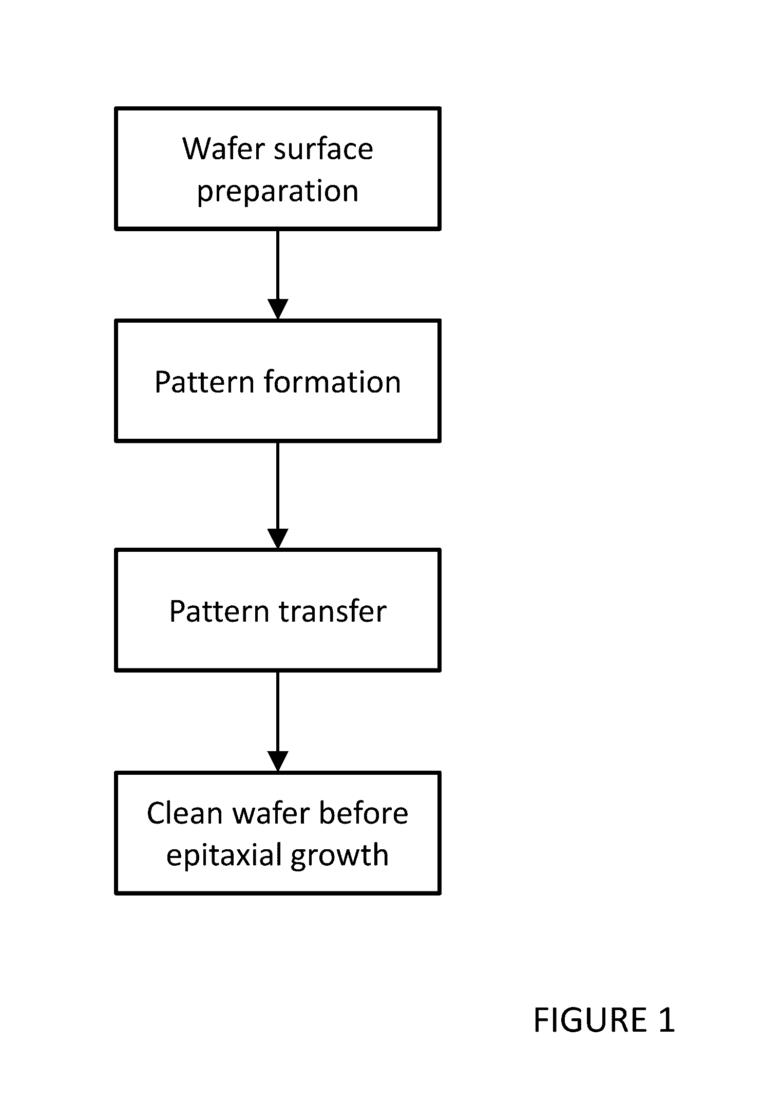
[0018]In the present invention, a fabrication process for epitaxy onto back-side patterned substrate, where the substrate patterns were defined prior to epitaxy and therefore simplify post growth processing. Specifically, for LED devices, said fabrication process reduces the post growth processing steps required to obtain high LEE due to strong scattering of the back-side features defined on the substrate. The features defined on the back-side patterned substrate scatters strongly with light emitted from the LED devices. Methods of obtaining such features include wet and dry etching.

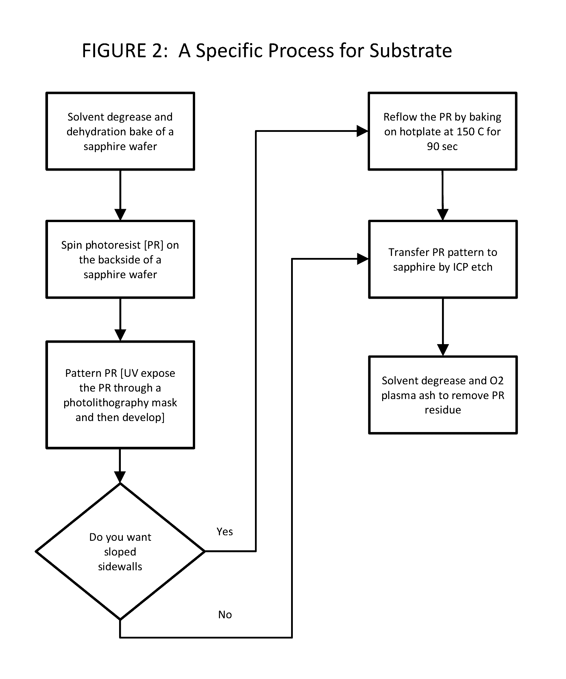
[0019]In an example, the present invention is described below. A process of manufacturing UV-LEDs onto pre-defined, back-side patterned sapphire substrate is provided. In an example, the present process defines features on the back-side of sapphire substrate. “Back-side” refers to the opposite side of the sapphire substrate where the epi-layers will be grown onto. In an example, features that are going t...


PUM


Abstract

In the present invention, a fabrication process for epitaxy onto back-side patterned substrate, where the substrate patterns were defined prior to epitaxy and therefore simplify post growth processing. Specifically, for LED devices, said fabrication process reduces the post growth processing steps required to obtain high LEE due to strong scattering of the back-side features defined on the substrate. The features defined on the back-side patterned substrate scatters strongly with light emitted from the LED devices. Methods of obtaining such features include wet and dry etching.

Description

CROSS-REFERENCE TO RELATED APPLICATIONS[0001]This application is a continuation of Nonprovisional application Ser. No. 14 / 194,425, filed Feb. 28, 2014, which claims priority to U.S. Provisional Application No. 61 / 776,760, filed Mar. 11, 2013, commonly assigned, and hereby incorporated by reference herein.BACKGROUND OF THE INVENTION[0002]Light emitting diodes (LEDs) based on InAlGaN multiple quantum wells (MQWs) generally suffer from certain limitations in terms of energy efficiency to produce light. One limitation is to efficiently extract light generated in the MQWs from inside the LEDs to air. Due to the refractive index difference between the InAlGaN material and air, a majority of the photons generated inside the MQWs is usually trapped inside by total internal reflection (TIR) and cannot escape the LEDs. Such photons eventually are lost inside the LEDs due to intrinsic material losses and other absorption mechanisms.[0003]There has been various ways being developed to improve l...

Claims


Application Information

Patent Timeline
Patent Type & Authority Patents(United States)
IPC IPC(8): H01L21/00H01L33/58H01L33/32H01L33/06H01L33/00H01L33/20
CPCH01L33/0075H01L33/007H01L33/0025H01L33/06H01L33/325H01L33/58H01L33/20
Inventor LIAO, YITAOCOLLINS, DOUGLAS A.
Owner RAYVIO
Why Eureka
Try Eureka