Lateral epitaxial technique based longitudinal structure AlGaN/GaN HEMT device and manufacture method thereof

A vertical structure, lateral epitaxy technology, applied in semiconductor/solid-state device manufacturing, semiconductor devices, electrical components, etc., can solve problems such as lattice damage, large leakage, complexity, etc., to reduce the impact of leakage, reduce production costs, Effect of Simplified Growth Process

Active Publication Date: 2015-05-27
SUZHOU NENGWU ELECTRONICS TECH
View PDF3 Cites 5 Cited by
  • Summary
  • Abstract
  • Description
  • Claims
  • Application Information

AI Technical Summary

Problems solved by technology

[0007] (4) Using lateral epitaxial SiO 2 As a current blocking layer, it just stays in the simulation, and at the same time, it does not give a good solution to the gaps that appear during the lateral epitaxy growth process. Instead, it simply verifies certain feasibility through simulation, and there is no specific solution. Get the whole structure of the device and the model of device fabrication
[0008] However, regardless of the use of Mg ion implantation or doping, on the one hand, it will introduce lattice damage, especially for the current blocking layer, resulting in a large leakage. On the other hand, Mg has a strong memory effect, which has a great impact on the secondary epitaxy Diffusion
The leakage and current collapse effects caused by the lattice damage caused by Al ion implantation are particularly serious. The reason for this current collapse is mainly due to the defects introduced by Al implantation, and the lattice damage caused by Al implantation must be performed at a very high temperature. It can only be repaired, and the temperature is about 1350°C. It is more complicated and relatively expensive for industrial use. At the same time, the lattice damage caused by large-scale ion implantation has an impact on the crystal quality of the secondary epitaxy; at the same time, SiO 2 The current blocking layer does not give a specific device structure and avoids problems such as voids during the healing process caused by lateral epitaxial growth

Method used


Image

  • Lateral epitaxial technique based longitudinal structure AlGaN/GaN HEMT device and manufacture method thereof
  • Lateral epitaxial technique based longitudinal structure AlGaN/GaN HEMT device and manufacture method thereof
  • Lateral epitaxial technique based longitudinal structure AlGaN/GaN HEMT device and manufacture method thereof

Examples


Embodiment Construction

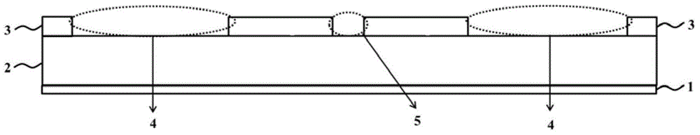
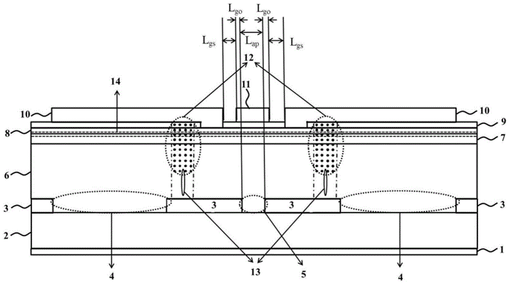
[0044] The embodiment of the present invention discloses a vertical structure AlGaN / GaN HEMT device based on lateral epitaxy technology, including a substrate and a current blocking layer formed on the substrate, and a current conduction layer is formed on the current blocking layer. The vertical structure AlGaN / GaN HEMT device further includes an epitaxial layer grown laterally on the current blocking layer.

[0045] Preferably, the epitaxial layer includes a healing intrinsic GaN layer, an intrinsic GaN layer and an intrinsic AlGaN layer sequentially formed on the current blocking layer; the vertical structure AlGaN / GaN HEMT device also includes the intrinsic The AlGaN layer forms a source electrode in ohmic contact, a gate electrode disposed on the intrinsic AlGaN layer through a passivation layer, and a drain electrode formed on the bottom surface of the substrate. The passivation layer material can be selected from but not limited to Al 2 o 3 , silicon nitride (SiN x )...


PUM


Abstract

The invention discloses a lateral epitaxial technique based longitudinal structure AlGaN / GaN HEMT device and a manufacture method thereof. The device comprises a substrate, a current blocking layer and an epitaxial layer, wherein the current blocking layer is formed on the substrate; the epitaxial layer laterally epitaxially grows on the current blocking layer; a current conducting through hole is formed in the current blocking layer. According to the invention, the current blocking layer acts as an insulation layer, so that the problems that the two-dimensional electron gas concentration, self-diffusion, high electricity leakage and the like are caused by ion implantation damage due to Mg doping, barrier height improvement by Mg ion implantation and formation of a similar insulation layer by Al ion implantation in a traditional technology can be solved; meanwhile, the defects of high cost, long time consumption, technology complexity and the like due to secondary epitaxial growth are also prevented; in addition, a clearance region formed by incomplete healing is isolated via F ion implantation, so that the clearance region is not involved in the device structure, and the problems of electric leakage and the like caused by the clearance region are relieved effectively.

Description

technical field [0001] The invention belongs to the technical field of semiconductors, in particular to a vertical structure AlGaN / GaN HEMT device based on lateral epitaxy technology and a manufacturing method thereof. Background technique [0002] The application of wide bandgap semiconductor materials (bandgap greater than 2.2eV) in optoelectronic devices and electronic devices has surpassed that of Si-based and GaAs-based devices. With large band gap and high bonding energy, III-V nitrides are suitable for high-frequency and high-power fields, such as wireless communication base stations, radar, automotive electronics, etc.; with their excellent chemical and thermal stability It is suitable for making electronic and optoelectronic devices with high temperature resistance and radiation resistance. There is an urgent demand for such devices in harsh environments such as aerospace, nuclear industry, and military electronics. In addition to the application of optoelectronic ...

Claims


Application Information

Patent Timeline
Patent Type & Authority Applications(China)
IPC IPC(8): H01L29/778H01L21/335
CPCH01L21/205H01L29/66431H01L29/778
Inventor 张宝顺孙世闯付凯蔡勇于国浩张志利宋亮
Owner SUZHOU NENGWU ELECTRONICS TECH
Why Eureka
Try Eureka