GaN-based vertical diode and preparation method thereof

A technology of vertical diodes and diodes, applied in the direction of diodes, semiconductor/solid-state device manufacturing, semiconductor devices, etc., can solve problems such as improving breakdown, increasing conduction voltage, and difficult realization of vertical GaN devices

Pending Publication Date: 2020-05-19
SOUTH UNIVERSITY OF SCIENCE AND TECHNOLOGY OF CHINA
View PDF7 Cites 2 Cited by
  • Summary
  • Abstract
  • Description
  • Claims
  • Application Information

AI Technical Summary

Problems solved by technology

However, it is difficult to implement in vertical GaN devices due to the great challenges of selective p-doping and its activation
There are generally the following methods: (i) field plate structure and its combination with deep trenches; (ii) high-re...

Method used


Image

  • GaN-based vertical diode and preparation method thereof
  • GaN-based vertical diode and preparation method thereof
  • GaN-based vertical diode and preparation method thereof

Examples


Embodiment Construction

[0034] In order to make the object, technical solution and advantages of the present invention clearer, the present invention will be further described in detail below in conjunction with specific embodiments and with reference to the accompanying drawings.

[0035] Example This example provides a method for preparing a GaN-on-GaN vertical diode

[0036] Such as Figure 1-7 As shown, it specifically includes the following steps:

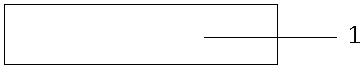
[0037] Step 1: If figure 1 As mentioned above, prepare a double-thrown n-type GaN substrate with a thickness of 400 μm and a substrate doping concentration of 1×10 18 cm -3 ;

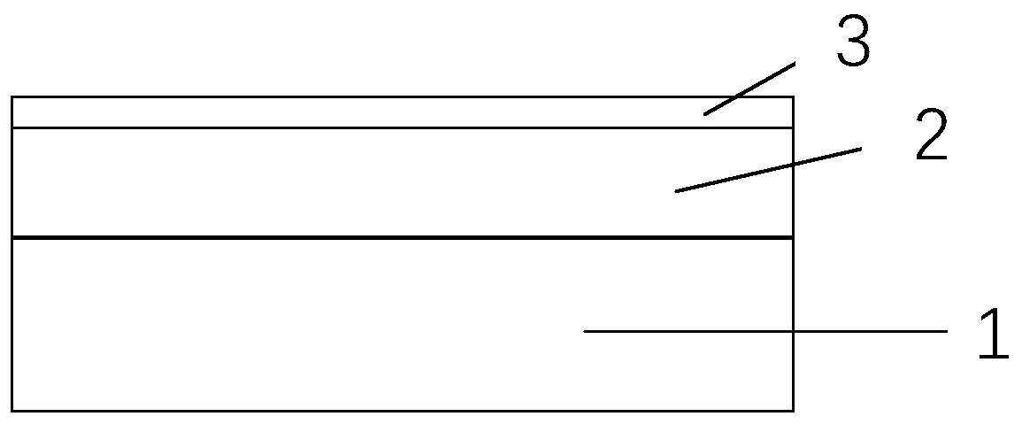
[0038] Step 2: If figure 2 The metal-organic chemical vapor deposition (MOCVD) method is used to grow a 11 μm n-type Si-doped GaN layer on a GaN substrate, and the doping concentration is about 1×10 16 6cm -3 , and then grow the n-AlGaN layer by MOCVD growth method, the thickness of n-AlGaN is 5nm, respectively choose ammonia gas, trimethylaluminum, trimethylgallium as...


PUM

PropertyMeasurementUnit
Doping concentrationaaaaaaaaaa
Thicknessaaaaaaaaaa
Thicknessaaaaaaaaaa

Abstract

The invention provides a GaN-based vertical diode and a preparation method thereof. The preparation method comprises the steps: S1, sequentially growing an n-GaN layer and an AlGaN layer on a GaN substrate; S2, growing a barrier layer on the AlGaN layer, etching the end part of the barrier layer and the end part of the AlGaN layer, and exposing the end part of the n-GaN layer; S3, sequentially injecting energy from low to high through oxygen ion injection, and forming a Ga2O3 high-resistance region at the end part of the n-GaN layer; S4, removing the barrier layer, and depositing an anode on the AlGaN layer; S5, depositing an oxide layer on the AlGaN layer, and forming a hole in the top of the oxide layer; and S6, depositing a cathode on the back surface of the GaN substrate. A large number of electrons are attracted through an oxygen ion implantation technology, so that an electric field is distributed more uniformly, the breakdown voltage is improved, a 5nm n-AlGaN thin layer grows epitaxially, the current transport capacity is enhanced through a polarization effect, and the SBD breakdown voltage is improved by adopting an oxide layer terminal structure.

Description

technical field [0001] The invention belongs to the field of semiconductor devices, in particular to a GaN-based vertical diode and a preparation method thereof. Background technique [0002] In vertical power rectifiers, GaN Schottky barrier diodes (SBDs) can provide low conduction / switching losses and high switching frequency due to their low forward voltage drop and fast reverse recovery characteristics. Meanwhile, GaN-on-GaN vertical devices can achieve high breakdown voltage (BV), high current capacity, low thermal resistance, and excellent dynamic performance, making them ideal for power electronics applications. Its structure and characteristics allow it to work stably in high-voltage, high-current output occasions and high-frequency environments. [0003] SBD has low power consumption, can operate at high voltage and high frequency, and has a small forward conduction voltage drop. It is mostly used in high-frequency, high-current rectifier diodes, freewheeling diode...

Claims


Application Information

Patent Timeline
IPC IPC(8): H01L21/329H01L29/872H01L29/06
CPCH01L29/0611H01L29/872H01L29/66212
Inventor 刘新科陈勇
Owner SOUTH UNIVERSITY OF SCIENCE AND TECHNOLOGY OF CHINA
Why Eureka
Try Eureka