GaN Schottky diode and fabrication method thereof

A gallium nitride Schottky technology and a manufacturing method are applied in the field of gallium nitride Schottky diode structure and its manufacturing, and can solve the problem that the Schottky barrier height cannot be effectively improved, the electron concentration is limited, and the breakdown voltage is increased. problem, to achieve the effect of reducing leakage current, increasing potential barrier height, and increasing breakdown voltage

Active Publication Date: 2017-07-14
JIANGSU CORENERGY SEMICON CO LTD
View PDF4 Cites 4 Cited by
  • Summary
  • Abstract
  • Description
  • Claims
  • Application Information

AI Technical Summary

Problems solved by technology

[0003] The disadvantage of the existing Gallium Nitride Schottky diode structure is that since the intrinsic Gallium Nitride is N-type, the electron concentration in the N-type GaN l

Method used


Image

  • GaN Schottky diode and fabrication method thereof
  • GaN Schottky diode and fabrication method thereof
  • GaN Schottky diode and fabrication method thereof

Examples


Example Embodiment

[0026] Below in conjunction with accompanying drawing and embodiment example, the present invention will be further described:

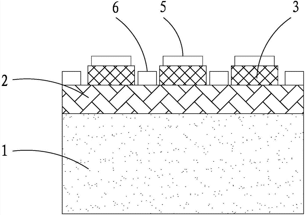
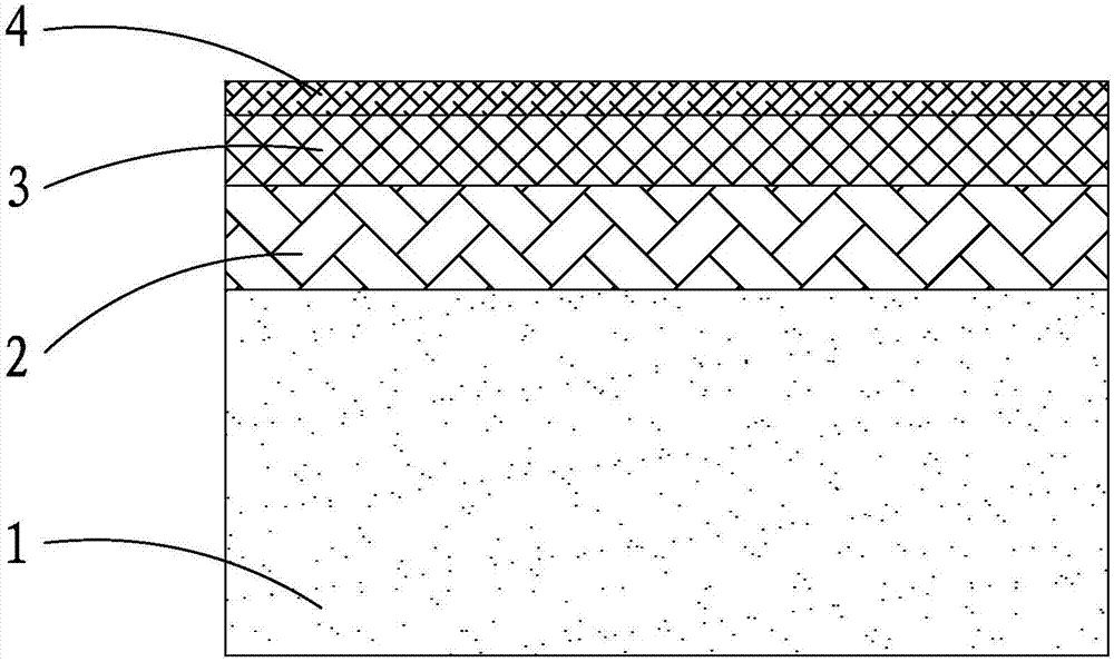
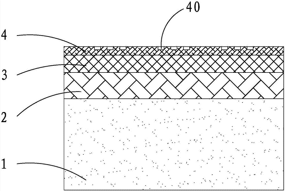
[0027] like Figure 5 Shown: a gallium nitride Schottky diode, including a substrate 1, an N+ gallium nitride layer 2 formed on the substrate 1, an N-gallium nitride layer 3 formed on the N+ gallium nitride layer 2 The mesa, the P-type GaN layer 4 with grooves 40 etched on the mesa of the N-GaN layer 3, the Schottky metal layer 5 formed on the P-GaN layer 4, and the N+GaN layer An ohmic metal layer 6 is formed on the 2, the Schottky metal layer 5 forms the anode of the diode, and the ohmic metal layer 6 forms the cathode of the diode.

[0028] The following describes in detail the fabrication method of the Gallium Nitride Schottky diode in this implementation, including the following steps:

[0029] (1), grow N+ gallium nitride layer 2 on sapphire, silicon or silicon carbide substrate 1, grow N-gallium nitride layer 3 on the surface of N+ gallium n...


PUM

PropertyMeasurementUnit
Thicknessaaaaaaaaaa
Growth thicknessaaaaaaaaaa

Abstract

The invention relates to a GaN Schottky diode. The GaN Schottky diode comprises a substrate, an N+ GaN layer, an N-GaN layer table surface and a P-type GaN layer, wherein grooves are etched in the P-type GaN layer, Schottky metal layers are formed on the P-type GaN layer and are used as positive electrodes, and ohmic metal layers are formed on the N+ GaN layer and are used as negative electrodes. A fabrication method of the GaN Schottky diode comprises the steps of sequentially growing the N+ GaN layer, the N-GaN layer and the P-type GaN layer on an upper surface of the substrate; forming the table surface with the P-type GaN layer and the N-GaN layer, and partially etching the P-type GaN layer on each table surface to form a series of grooves; and depositing the Schottky metal layers on the P-type GaN layer to used as the positive electrodes, and depositing the ohmic metal layers on the N+GaN layer to be used as the negative electrodes. By the GaN Schottky diode, carriers under a Schottky electrode can be consumed, the Schottky barrier height is increased, the leakage current is reduced, the breakdown voltage is increased, the grooves under the Schottky electrode can be used for reducing the positive conduction voltage, so that the positive characteristic and the negative characteristic of the device are simultaneously improved.

Description

technical field [0001] The invention relates to the field of semiconductors, in particular to a gallium nitride Schottky diode structure and a manufacturing method thereof. Background technique [0002] In the prior art, the structure of GaN Schottky diode is as follows figure 1 Shown: N+GaN layer 2 and N-GaN layer 3 are grown on sapphire, silicon or SiC substrate 1, N-GaN layer 3 is etched to N+GaN layer 2, and N-GaN layer A Schottky metal layer 5 is deposited on the GaN layer 3 as an anode, and an ohmic metal layer 6 is deposited on the N+GaN layer 2 as a cathode, thereby forming a Schottky diode. [0003] The disadvantage of the existing Gallium Nitride Schottky diode structure is that since the intrinsic Gallium Nitride is N-type, the electron concentration in the N-type GaN layer is limited by doping during the growth process, so it cannot be effectively Increase the Schottky barrier height to achieve the purpose of reducing leakage current and increasing breakdown vo...

Claims


Application Information

Patent Timeline
IPC IPC(8): H01L29/872H01L29/06H01L29/20H01L21/329
CPCH01L29/0607H01L29/0684H01L29/2003H01L29/66143H01L29/872
Inventor 张葶葶朱廷刚李亦衡王东盛苗操魏鸿源严文胜
Owner JIANGSU CORENERGY SEMICON CO LTD
Why Eureka
Try Eureka