Light-emitting diode epitaxial structure growth method

A technology of light-emitting diodes and epitaxial structures, which is applied in the direction of electrical components, circuits, semiconductor devices, etc., can solve the problems of light-emitting diodes such as the decline in luminous efficiency, and achieve the effects of reducing polarization effects, preventing electron overflow, and enhancing barrier heights

Active Publication Date: 2020-03-24
宁波安芯美半导体有限公司
View PDF12 Cites 4 Cited by
  • Summary
  • Abstract
  • Description
  • Claims
  • Application Information

AI Technical Summary

Problems solved by technology

[0005] In view of the above-mentioned shortcomings of the prior art, the object of the present invention is to provide a method for growing an epitaxial structure of a light-emitting diode, which is used to solve the problem of the decrease of the luminous efficiency of the light-emitting diode in the prior art

Method used


Image

  • Light-emitting diode epitaxial structure growth method
  • Light-emitting diode epitaxial structure growth method
  • Light-emitting diode epitaxial structure growth method

Examples


Embodiment Construction

[0041] The implementation of the present invention will be illustrated by specific specific examples below, and those skilled in the art can easily understand other advantages and effects of the present invention from the contents disclosed in this specification.

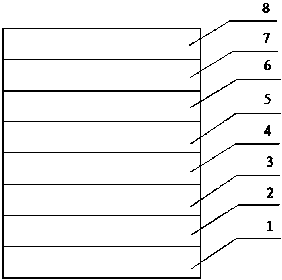
[0042] see Figure 1 to Figure 5 . It should be noted that the structures, proportions, sizes, etc. shown in the drawings attached to this specification are only used to match the content disclosed in the specification, for those who are familiar with this technology to understand and read, and are not used to limit the implementation of the present invention. Limiting conditions, so there is no technical substantive meaning, any modification of structure, change of proportional relationship or adjustment of size, without affecting the effect and purpose of the present invention, should still fall within the scope of the present invention. The disclosed technical content must be within the scope covered. At the sa...


PUM

PropertyMeasurementUnit
thicknessaaaaaaaaaa
thicknessaaaaaaaaaa
thicknessaaaaaaaaaa

Abstract

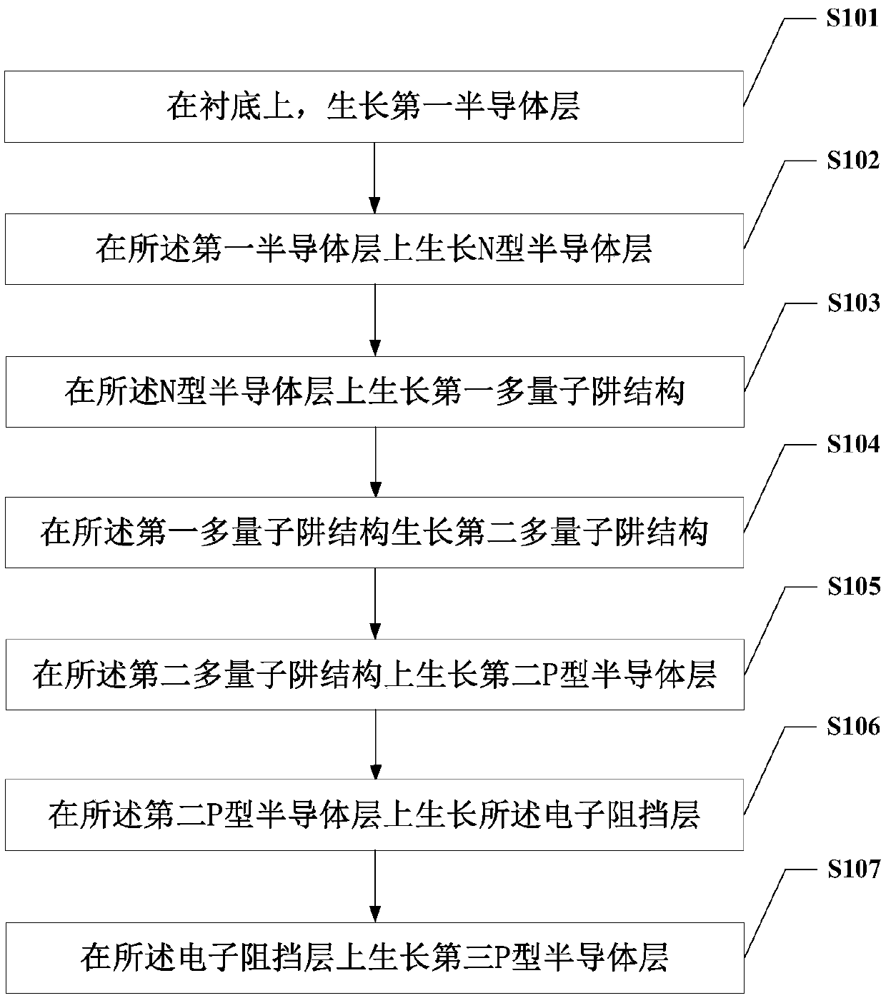
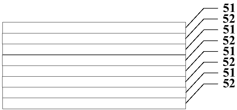
The invention provides a light-emitting diode epitaxial structure growth method, which comprises the following steps of: growing a first semiconductor layer on a substrate; growing an N-type semiconductor layer on the first semiconductor layer; growing a first multi-quantum well structure on the N-type semiconductor layer; growing a second multi-quantum well structure on the first multi-quantum well structure, wherein the second multi-quantum well structure at least comprises at least two multi-quantum wells and a multi-quantum potential barrier, the multi-quantum potential barrier comprises afirst nitride containing aluminum and gallium and a second nitride containing aluminum, and the first nitride and the second nitride grow alternately; growing a second P-type semiconductor layer on the second multi-quantum well structure; growing the electron blocking layer on the second P-type semiconductor layer; and growing a third P-type semiconductor layer on the electron blocking layer.

Description

technical field [0001] The invention relates to the technical field of epitaxial structures of light emitting diodes, in particular to a method for growing epitaxial structures of light emitting diodes. Background technique [0002] A light-emitting diode (LED, Light Emitting Diode) is a semiconductor solid-state light-emitting device, which uses a semiconductor PN junction as a light-emitting material, and can directly convert electricity into light. [0003] Ultraviolet LED, referred to as UV-LED, refers to the LED with a light emitting wavelength of 200nm-400nm. Ultraviolet LED has many advantages such as small size, long life, environmental protection and low voltage power supply, and has become a better alternative to mercury lamps as a new generation of ultraviolet light sources. choose. Although ultraviolet LEDs have many excellent characteristics, the luminous efficiency and overall performance of ultraviolet LEDs are lower than those of blue LEDs, especially for UV...

Claims


Application Information

Patent Timeline
Patent Type & Authority Applications(China)
IPC IPC(8): H01L33/00H01L33/06H01L33/32
CPCH01L33/0075H01L33/06H01L33/32
Inventor 唐军吴礼清
Owner 宁波安芯美半导体有限公司
Why Eureka
Try Eureka