

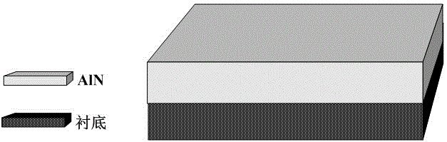
Preparation method of aluminum nitride monocrystalline film
A technology of single crystal thin film and aluminum nitride, which is applied in semiconductor/solid-state device manufacturing, electrical components, circuits, etc., can solve the problems of high energy consumption and cost, high growth temperature, etc., and achieve reduced growth cost, low growth temperature, The effect of simple growth process
- Summary
- Abstract
- Description
- Claims
- Application Information
AI Technical Summary
Problems solved by technology
Method used
Image

Examples
Embodiment Construction
[0023] Below in conjunction with the accompanying drawings, the present invention will be further described through implementation examples.
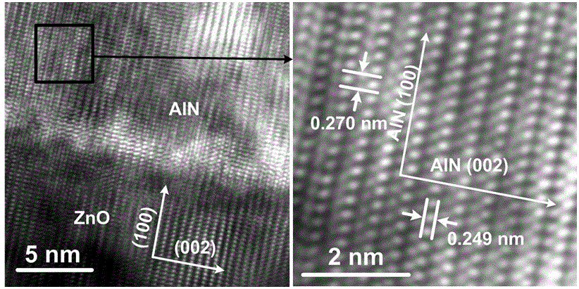
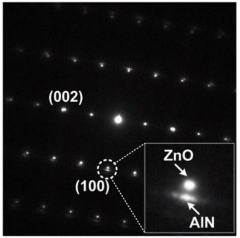
[0024] Clean the ZnO (100) single wafer, the steps are as follows: first rinse with deionized water to remove possible adhered dust particles; put in acetone solution for 180 s to remove organic matter that may exist on the surface; put in absolute ethanol solution for 180 s, Remove the acetone solution and organic impurities adhering to the surface; rinse the ZnO single wafer with deionized water and dry it with high-purity nitrogen for later use.
[0025] AlN thin films were grown on ZnO single wafers by thermal ALD technique. Using TMA and high-purity NH 3 As the reaction source, the temperature of the source was set at 20° C., the growth temperature was 360° C., and the reaction base pressure was 1 Torr. A standard ALD growth cycle of AlN is as follows: TMA is fed into the reaction chamber with a pulse time of 0.2 s; argon gas is ...
PUM
| Property | Measurement | Unit |
|---|---|---|
| thickness | aaaaa | aaaaa |
| thickness | aaaaa | aaaaa |
Abstract
Description
Claims
Application Information