

GaN film growing on magnesium aluminate scandium substrate as well as preparation method and application of GaN film
A magnesium-scandium aluminate and substrate technology, which is applied in the field of GaN thin film and its preparation, can solve the problems affecting the performance of GaN-based devices, reducing the carrier mobility of materials, and reducing the quantum efficiency of devices, so as to achieve mature production technology, The effect of reducing production cost and relieving stress
- Summary
- Abstract
- Description
- Claims
- Application Information
AI Technical Summary
Problems solved by technology
Method used
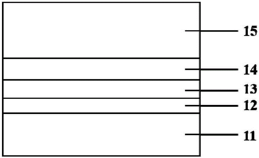
Image

Examples
Embodiment 1
[0037] A method for preparing a high-quality GaN film grown on a magnesium-scandium aluminate substrate, comprising the following steps:
[0038] (1) Selection of substrate and its crystal orientation: using ScMgAlO 4 The substrate, with the (0001) plane offset from the (11-20) plane by 0.5° as the epitaxial plane, the crystal epitaxial orientation relationship is: the (0001) plane of GaN is parallel to ScMgAlO 4 (0001) face;
[0039] (2) Substrate annealing treatment: the magnesium scandium aluminate substrate was annealed at 600 ° C for 1 hour in the molecular beam epitaxy vacuum growth chamber of the substrate to obtain an atomically flat surface;
[0040] (3) Epitaxial growth of GaN buffer layer: the substrate temperature is adjusted to 450°C, and the pressure of pulsed laser deposition in the reaction chamber is 2.0×10 -5 Pa, laser energy density is 1.8J / cm 2 A 30nm-thick GaN buffer layer was grown under conditions;
[0041] (4) Epitaxial growth of the GaN nucleation ...
Embodiment 2
[0051] The preparation method of the GaN film grown on the magnesium scandium aluminate substrate comprises the following steps:
[0052] (1) Selection of substrate and its crystal orientation: using ScMgAlO 4 The substrate, with the (0001) plane offset from the (11-20) direction by 0.5° as the epitaxial plane, the crystal epitaxial orientation relationship is: the (0001) plane of GaN is parallel to ScMgAlO 4 (0001) face;
[0053] (2) Substrate annealing treatment: the magnesium scandium aluminate substrate was annealed at 700°C for 2 hours in the molecular beam epitaxy vacuum growth chamber of the substrate to obtain an atomically flat surface;
[0054] (3) Epitaxial growth of GaN buffer layer: the substrate temperature is adjusted to 500°C, and the pressure in the reaction chamber is 3.0×10 by pulsed laser deposition. -5 Pa, laser energy density is 2.0J / cm 2 An 80nm-thick GaN buffer layer is grown under conditions;
[0055] (4) Epitaxial growth of the GaN nucleation laye...
PUM
| Property | Measurement | Unit |
|---|---|---|
| thickness | aaaaa | aaaaa |
| thickness | aaaaa | aaaaa |
| thickness | aaaaa | aaaaa |
Abstract
Description
Claims
Application Information