Method for preparing ZnO (zinc oxide)-based thin film transistor by using metal organic chemical vapor deposition

A metal-organic chemistry, thin-film transistor technology, applied in the field of microelectronics, can solve the problems of complex ZnO thin-film transistor process, low ZnO crystal quality, affecting device characteristics, etc.

Inactive Publication Date: 2010-06-16
JILIN UNIV
View PDF2 Cites 5 Cited by
  • Summary
  • Abstract
  • Description
  • Claims
  • Application Information

AI Technical Summary

Problems solved by technology

But both have certain shortcomings: the mobility of amorphous silicon TFT is low, and there is a problem of threshold drift with the increase of working time; polysilicon TFT has poor uniformity due to process reasons, and the manufacturing cost is high
However, the quality of ZnO crystals prepared by sputtering is not high, which affects the device characteristics.
However, the process of preparing ZnO thin film transistors by sputtering and other methods is complicated.

Method used


Image

  • Method for preparing ZnO (zinc oxide)-based thin film transistor by using metal organic chemical vapor deposition
  • Method for preparing ZnO (zinc oxide)-based thin film transistor by using metal organic chemical vapor deposition
  • Method for preparing ZnO (zinc oxide)-based thin film transistor by using metal organic chemical vapor deposition

Examples


Embodiment 1

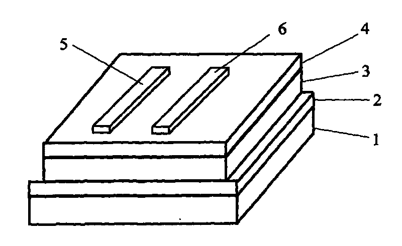
[0024] 1. Select ITO glass as the substrate 1, transparent and conductive ITO film as the gate 2, and chemically clean the substrate. The steps are: ultrasonic cleaning with toluene for 5 minutes, ultrasonic cleaning with acetone for 5 minutes, and ultrasonic cleaning with ethanol for 5 minutes, and then Recirculate once, rinse with deionized water, dry with high-purity nitrogen and set aside;

[0025] 2. Use the MOCVD method on the processed substrate, especially the special growth MOCVD equipment described in ZL 02100436.6 and ZL200410011164.0 patents, use magnesium dicene as the magnesium source, and the magnesium source is carried into the reaction chamber with argon gas. Chemically react with high-purity oxygen at 650°C to epitaxially grow the MgO insulating layer 3 , the flow rate of argon gas is 20 sccm, the flow rate of oxygen gas is 200 sccm, the pressure of the reaction chamber is 150 Pa, and the layer thickness is 200 nanometers. Then continue to adopt the above-men...

Embodiment 2

[0028] The difference between this embodiment and embodiment 1 is that the substrate 1 adopts a resistivity of 10 -3 The silicon substrate of Ω cm is also used as the gate electrode 2 of the transistor, and the others are the same as in embodiment 1, that is, the Al 2 o 3 , MgO or Mg with Mg content (y=0.9) y Zn 1-y O insulating layer 3, prepared Al 2 o 3 The organic source that adopts can be trimethylaluminum, and oxygen source is high-purity oxygen, and flow rate is respectively 2sccm and 200sccm; Preparation Mg y Zn 1-y The organic source used for O is diethylzinc and dichloromagnesium, the oxygen source is high-purity oxygen, and the oxygen flow rate is 200 sccm. The organic source is carried into the reaction chamber by argon gas. The temperature is 650°C, the pressure of the reaction chamber is about 150Pa during growth, and the layer thickness is about 500nm, and then MOCVD is used to grow ZnO or Mg with low Mg (x=0.1) content x Zn 1-X O active channel layer 4, ...

Embodiment 3

[0030] The difference between this embodiment and Embodiment 1 is that the substrate 1 is made of glass, and the gate electrode 2 is a ZnO-doped Ga transparent conductive film grown by MOCVD, and the others are the same as in Embodiment 1; , the insulating layer 3 and the ZnO-based active channel layer 4 are all grown by MOCVD technology, and the material growth of each layer can be completed at one time in the MOCVD growth equipment.


PUM


Abstract

The invention belongs to the field of microelectronic technology, particularly relates to a method for preparing a zinc oxide (ZnO)-based thin film transistor (TFT) by using organic chemical vapor deposition (MOCVD). The ZnO-based thin film transistor consists of a lining, a grid, an insulating layer, a ZnO based active channel layer, a source electrode and a drain electrode, wherein the insulating layer and the ZnO based active channel layer both adopt the MOCVD technology to finish the growth of materials, and compared with other extension technologies, the MOCVD technology has the advantage that a prepared semiconductor material has higher quality. The growth of material in all layers is finished in one step in MOCVD growth equipment, thereby the material growth process is greatly simplified, and the thickness of each layer of semiconductor material can be accurately controlled. The invention provides the process method for growing the ZnO-based TFT by adopting the MOCVD growth equipment suitable for industrial production, solves the key problems that the prepared ZnO-based TFT has low quality by using other methods, and the like, and prepares the ZnO-based TFT with higher quality.

Description

technical field [0001] The invention belongs to the technical field of microelectronics, and in particular relates to a metal organic chemical vapor deposition (MOCVD) preparation method of a zinc oxide (ZnO)-based thin film transistor (TFT). Background technique [0002] With the advent of the information age, flat-panel display devices as information terminals have the characteristics of complete flatness, lightness, thinness, and power saving, which is in line with the inevitable trend of future image display development. Actively driven flat panel display technology is widely used in various consumer electronic products, among which the most representative ones are thin film transistor driven liquid crystal display (TFT-LCD) and organic light emitting display (TFT-OLED). With the large-scale commercial use of 3G worldwide, TFT display screens will usher in a rare opportunity for development. [0003] Traditional thin film transistors usually use Si materials, including ...

Claims


Application Information

Patent Timeline
Patent Type & Authority Applications(China)
IPC IPC(8): H01L21/336
Inventor 杜国同赵旺夏晓川李万程张宝林
Owner JILIN UNIV
Why Eureka
Try Eureka