Electronic component embedded substrate and manufacturing method thereof

a technology of embedded substrate which is applied in the direction of final product manufacturing, printed electric component incorporation, printed circuit non-printed electric components, etc., can solve the problems of serious problems such as the matching error of vias and electronic components, and achieve the effect of improving the electrical connectivity of electronic components embedded in substrates

Active Publication Date: 2016-10-04
SAMSUNG ELECTRO MECHANICS CO LTD
View PDF60 Cites 12 Cited by
  • Summary
  • Abstract
  • Description
  • Claims
  • Application Information

AI Technical Summary

Benefits of technology

[0014]The present invention has been invented in order to overcome the above-described problems and it is, therefore, an object of the present invention to provide an electronic component embedded substrate that can improve electrical connectivity of an electronic component embedded in a substrate.
[0015]Further, it is another object of the present invention to provide an electronic component embedded substrate that can improve electronic connectivity of an electronic component embedded in a substrate.

Problems solved by technology

However, since the size of the via contact should be reduced according to a reduction in the size of the electronic component, as the electronic component becomes smaller, a matching error of the via and the electronic component is emerged as a serious problem.

Method used


Image

  • Electronic component embedded substrate and manufacturing method thereof
  • Electronic component embedded substrate and manufacturing method thereof
  • Electronic component embedded substrate and manufacturing method thereof

Examples


Embodiment Construction

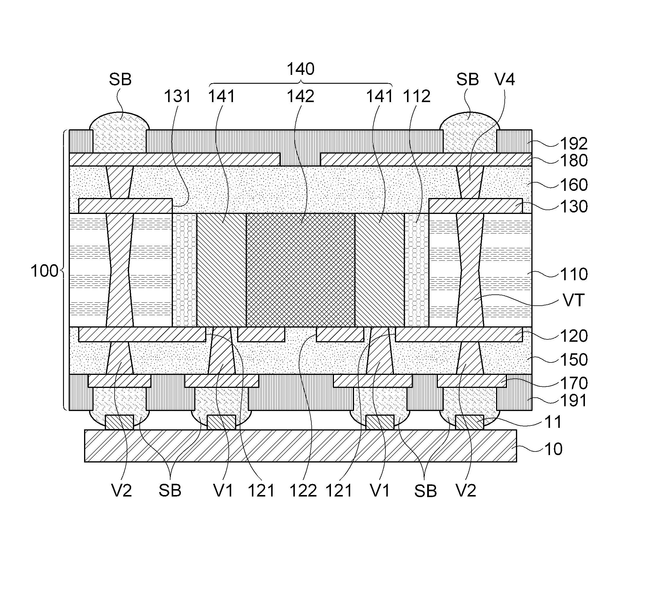
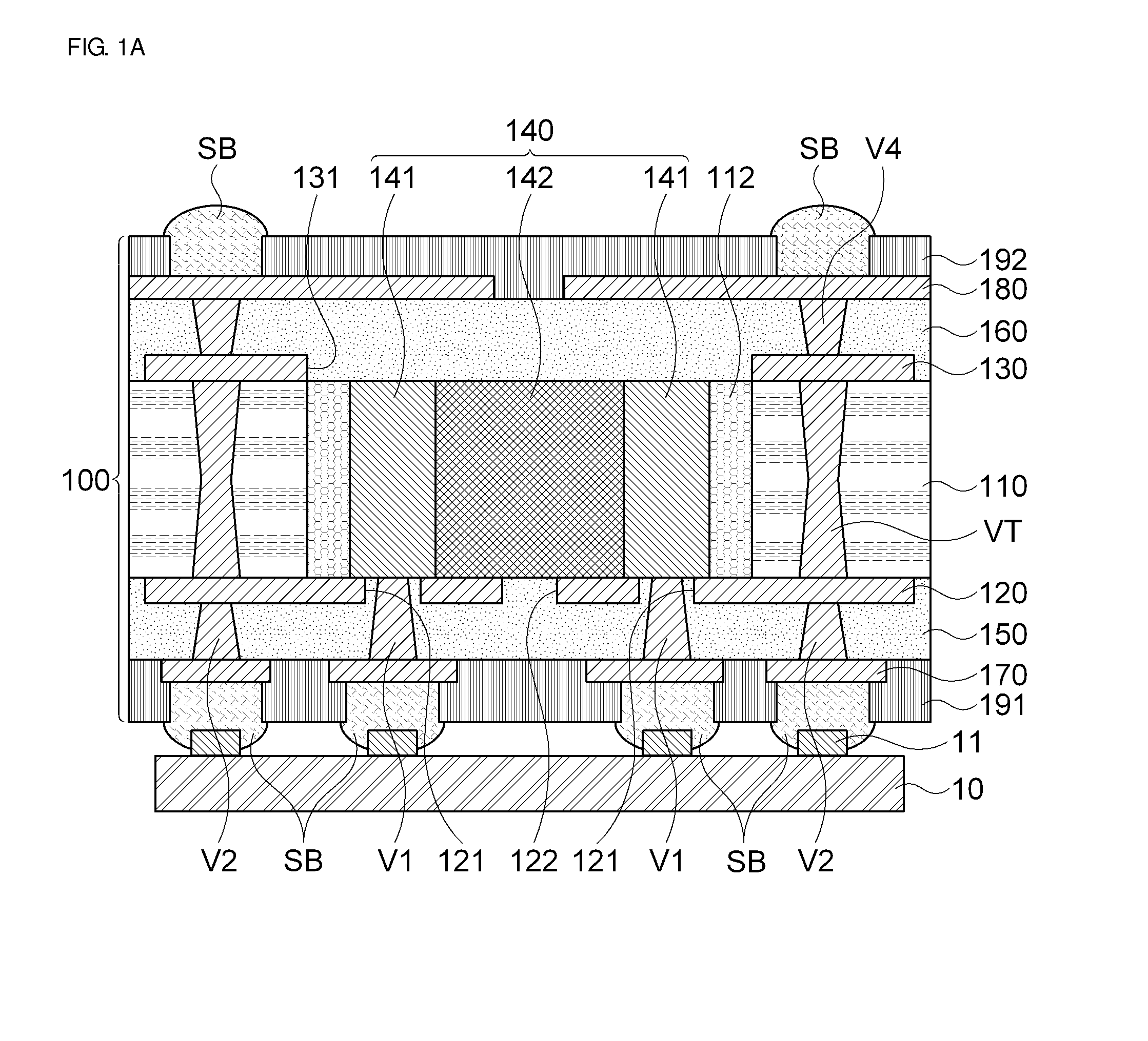
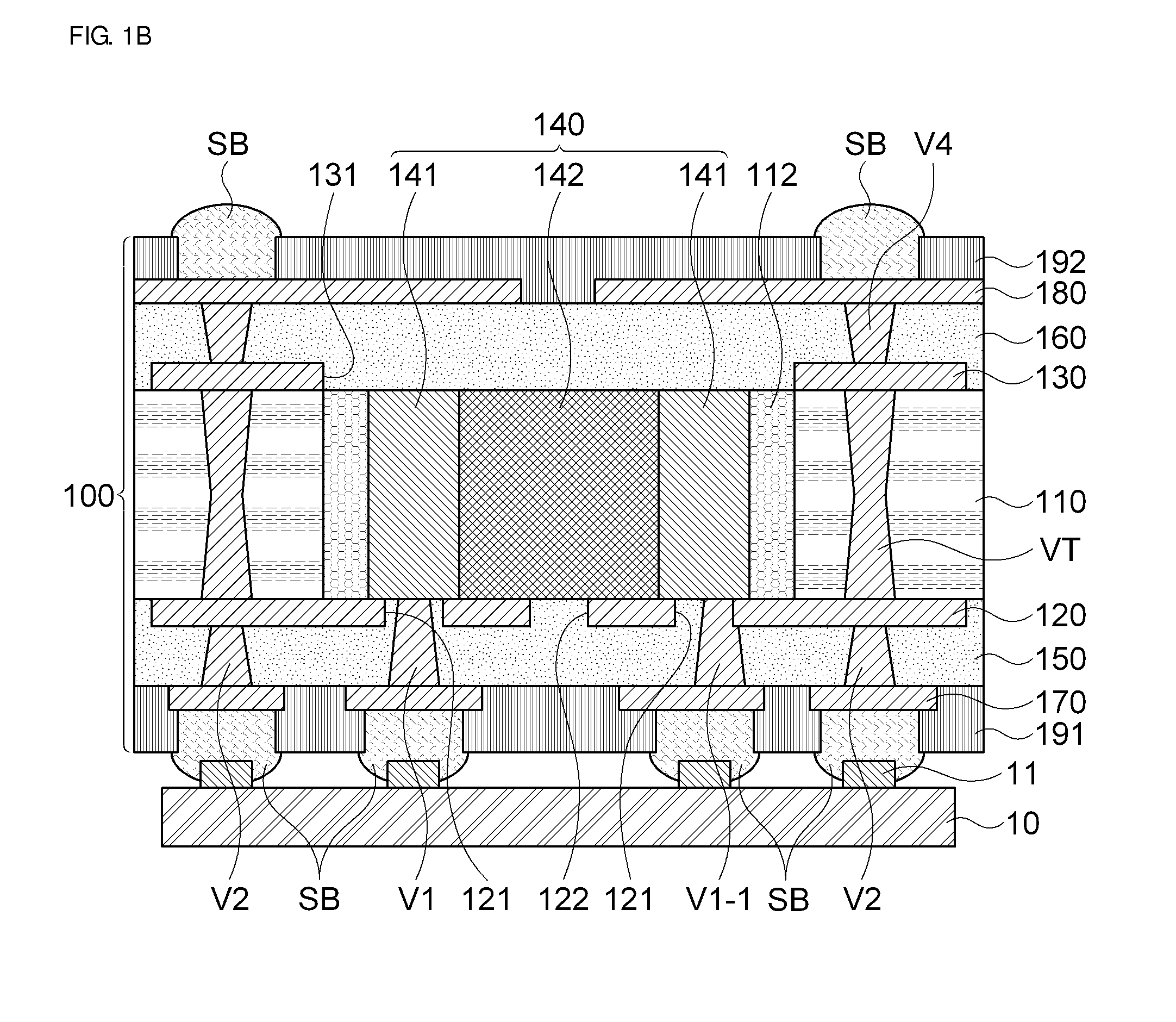
[0063]Advantages and features of the present invention and methods of accomplishing the same will be apparent by referring to embodiments described below in detail in connection with the accompanying drawings. However, the present invention is not limited to the embodiments disclosed below and may be implemented in various different forms. The embodiments are provided only for completing the disclosure of the present invention and for fully representing the scope of the present invention to those skilled in the art. Like reference numerals refer to like elements throughout the specification.

[0064]Terms used herein are provided to explain embodiments, not limiting the present invention. Throughout this specification, the singular form includes the plural form unless the context clearly indicates otherwise. When terms “comprises” and / or “comprising” used herein do not preclude existence and addition of another component, step, operation and / or device, in addition to the above-mentione...


PUM

PropertyMeasurementUnit
sizeaaaaaaaaaa
sizeaaaaaaaaaa
sizeaaaaaaaaaa

Abstract

The present invention relates to an electronic component embedded substrate including: a first insulating layer including a cavity; an electronic component inserted in the cavity; a first metal pattern formed on a lower surface of the first insulating layer to mount the electronic component thereon and including at least one guide hole for exposing a portion of the external electrode; a second insulating layer formed on the lower surface of the first insulating layer to cover the first metal pattern; a first circuit pattern formed on a lower surface of the second insulating layer; and a first via for electrically connecting the first external electrode exposed through the guide hole and the first circuit pattern, and can improve electrical connectivity between the external electrode and the via even when the size of the external electrode of the electronic component is reduced than before.

Description

CROSS-REFERENCE TO RELATED APPLICATIONS[0001]This application claims the foreign priority benefit under 35 U.S.C. Section 119 of Korean Patent Application Serial No. 10-2012-0137048, filed Nov. 29, 2012, which is hereby incorporated by reference in its entirety into this application.BACKGROUND OF THE INVENTION[0002]1. Field of the Invention[0003]The present invention relates to an electronic component embedded substrate.[0004]2. Description of the Related Art[0005]As the recently released mobile devices such as smartphones and tablet PCs have been dramatically improved in performance and demanded to have high portability, studies on miniaturization, slimming, and high performance of electronic components used in these mobile devices have been continuously made.[0006]Here, since an electronic component embedded substrate disclosed in Patent Document 1 etc. can secure a space for mounting extra components on its surface by embedding electronic components in a substrate, it has been hi...

Claims


Application Information

Patent Timeline
Patent Type & Authority Patents(United States)
IPC IPC(8): H05K1/16H05K1/18H05K3/46
CPCH05K1/186H05K2201/10015H05K2201/10636Y02P70/611Y10T29/4913H01L2924/15311H05K3/4644H05K3/4697Y02P70/50H05K1/18H05K3/46
Inventor CHUNG, YUL KYOLEE, DOO HWANLEE, SEUNG EUNSHIN, YEE NA
Owner SAMSUNG ELECTRO MECHANICS CO LTD
Why Eureka
Try Eureka