Resilient conductive electrical interconnect

a resilient, conductive technology, applied in the direction of coupling device connection, coupling device details, printed circuit manufacture, etc., can solve the problems of reducing the surface area available for placing a contact, limiting the space available for locating resilient contact members, reducing the electrical performance of the connection, etc., to reduce parasitic electrical effects and impedance mismatch, increase current carrying capacity, and enhance electrical performance

Active Publication Date: 2012-02-23
HSIO TECH
View PDF4 Cites 73 Cited by
  • Summary
  • Abstract
  • Description
  • Claims
  • Application Information

AI Technical Summary

Benefits of technology

[0023]The present disclosure is also directed to several additive processes that combine the mechanical or structural properties of a polymer material, while adding metal materials in an unconventional fashion, to create electrical paths that are refined to provide electrical performance improvements. By adding or arranging metallic particles, conductive inks, plating, or portions of traditional alloys, the composite contact structure reduces parasitic electrical effects and impedance mismatch, potentially increasing the current carrying capacity.
[0024]The use of additive printing processes permits the material set in a given layer to vary. Traditional PCB and flex circuit fabrication methods take sheets of material and stack them up, laminate, and/or drill. The materials in each layer are limited to the materials in a particular sheet. Additive printing technologies permit a wide variety of materials to be applied on a layer with a registration relative to the features of the previous layer. Selective addition of conductive, non-conductive, or semi-conductive materials at precise locations to create a desired effect has the major advantages in tuning impedance or adding electrical function on a given layer. Tuning performance on a layer by layer basis relative to the previous layer greatly enhances electrical performance.
[0025]The present interconnect assembly can serve as a platform to add passive and active circuit features to improve electrical performance or internal function and intelligence. Passive circuit features refer to a structure having a desired electrica

Problems solved by technology

As the terminal pitch reduces, however, the surface area available to place a contact is also reduced, which limits the space available to locate resilient contact members that can deflect without shorting to an adjacent contact member.
Long contact members, however, tend to reduce the electrical performance of the connection by creating a parasitic effect that impacts the signal as it travels through the contact.
Long contact members also require thinner walls in the housing in order to meet pitch requirements,

Method used


Image

  • Resilient conductive electrical interconnect
  • Resilient conductive electrical interconnect
  • Resilient conductive electrical interconnect

Examples


Embodiment Construction

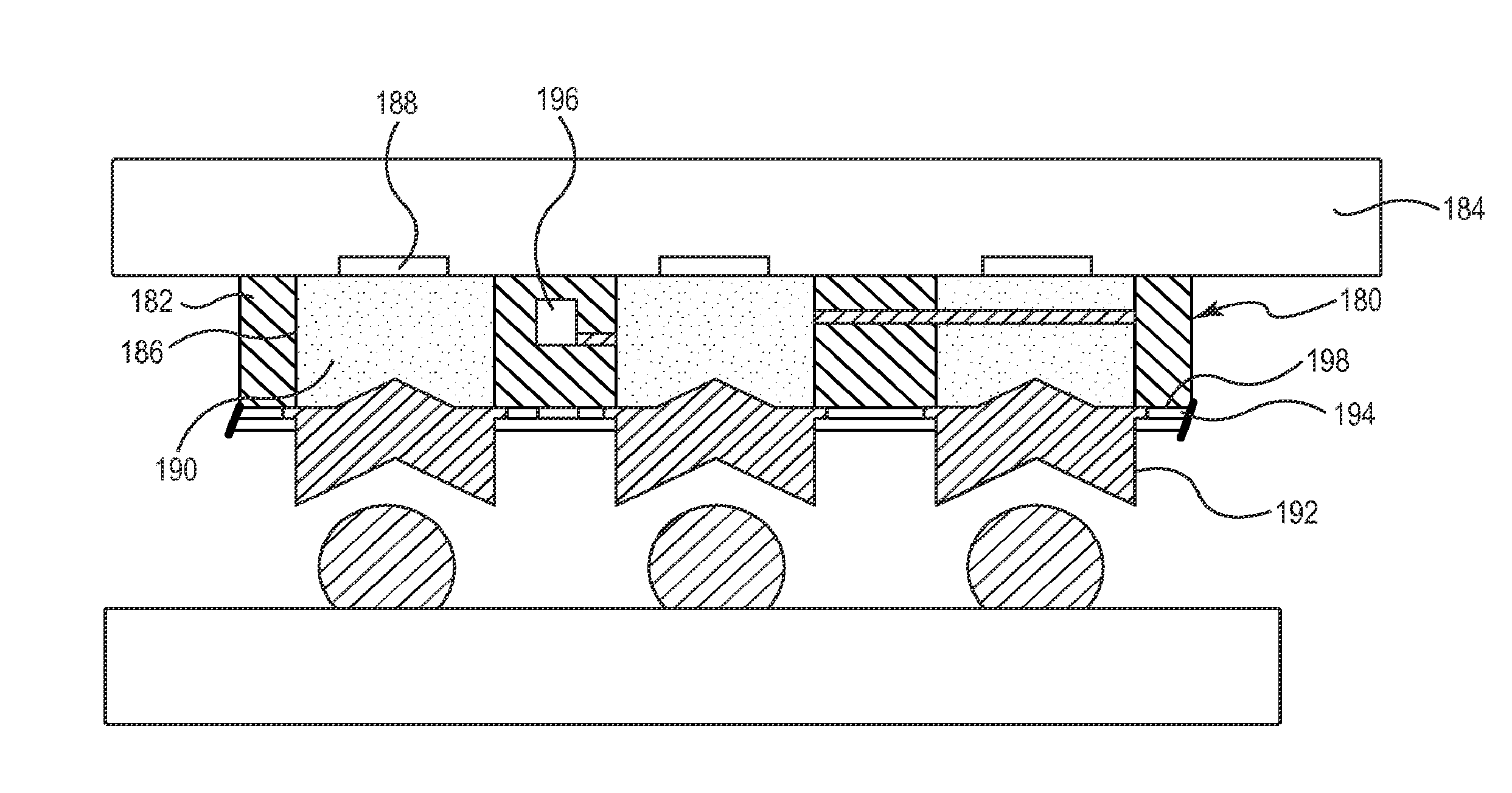
[0037]An interconnect assembly, according to the present disclosure, may permit fine contact-to-contact spacing (pitch) on the order of less than 1.0 pitch, and more preferably a pitch of less than about 0.7 millimeter, and most preferably a pitch of less than about 0.4 millimeter. Such fine pitch interconnect assemblies are especially useful for communications, wireless, and memory devices. The disclosed low cost, high signal performance interconnect assemblies, which have low profiles and can be soldered to the system PC board, are particularly useful for desktop and mobile PC applications.

[0038]The disclosed interconnect assemblies permit IC devices to be installed and uninstalled without the need to reflow solder. The solder-free electrical connection of the IC devices is environmentally friendly. In another embodiment, the interconnect assembly can be formed directly on one of the circuit members.

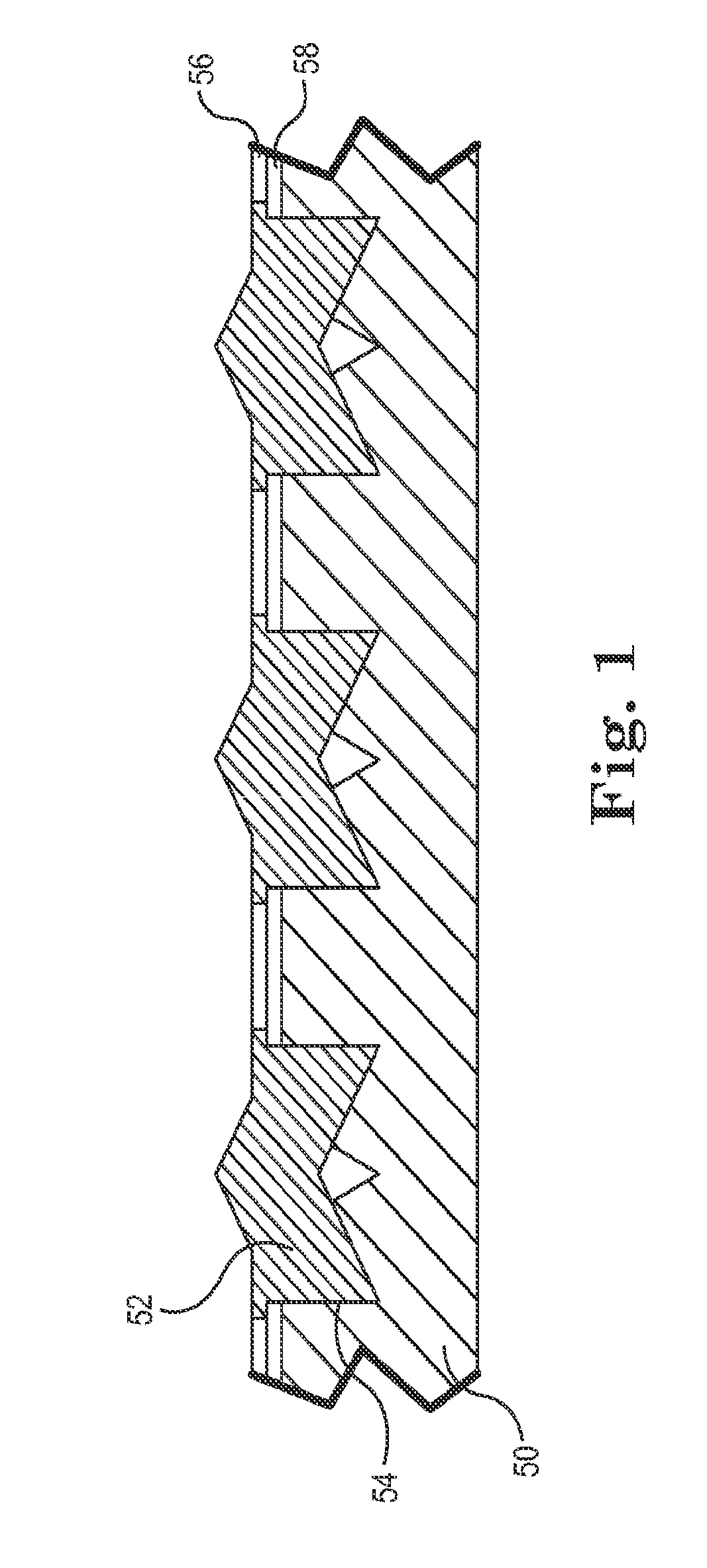
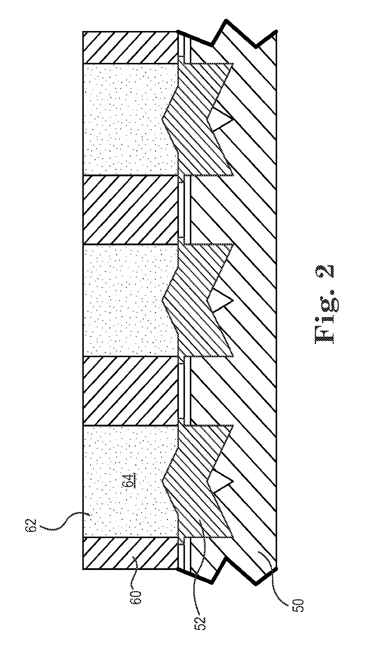
[0039]FIG. 1 is a side cross-sectional view of a portion of a carrier 50 with an a...


PUM

PropertyMeasurementUnit
Moldableaaaaaaaaaa
Shapeaaaaaaaaaa
Electrical conductoraaaaaaaaaa

Abstract

An interconnect assembly including a resilient material with a plurality of through holes extending from a first surface to a second surface. A plurality of discrete, free-flowing conductive particles is located in the through holes. The conductive particles are preferably substantially free of non-conductive materials. A plurality of first contact tips are located in the through holes adjacent the first surface and a plurality of second contact tips are located in the through holes adjacent the second surface. The resilient material provides the required resilience, while the conductive particles provide a conductive path substantially free of non-conductive materials.

Description

TECHNICAL FIELD[0001]The present application relates to a high performance electrical interconnect between circuit members, such as integrated circuits, printed circuit assemblies (PCA), and the like. The present interconnect can also be formed directly on a circuit member.BACKGROUND OF THE INVENTION[0002]Traditional IC sockets are generally constructed of an injection molded plastic insulator housing which has stamped and formed copper alloy contact members stitched or inserted into designated positions within the housing. These contact members can be in a flat or “blank” format, or they can be produced with a series of forms, bends, and features to accommodate a desired function such as retention within the plastic housing.[0003]The designated positions in the insulator housing are typically shaped to accept and retain the contact members. The assembled socket body is then generally processed through a reflow oven which melts and attaches solder balls to the base of the contact me...

Claims


Application Information

Patent Timeline
IPC IPC(8): H05K1/11H05K3/30
CPCH01R13/2414Y10T29/49139H01R13/2485
Inventor RATHBURN, JAMES
Owner HSIO TECH
Why Eureka
Try Eureka