Compliant printed circuit peripheral lead semiconductor package

a technology of semiconductor packaging and printed circuit, which is applied in the field of no lead ic packaging, can solve the problems of device not being connected to the final pcb, size and distance between die terminals being so small, and reducing so as to improve mechanical performance of the circuit, reduce environmental problems, and reduce parasitic electrical effects and impedance mismatch

Inactive Publication Date: 2012-02-23
HSIO TECH
View PDF4 Cites 56 Cited by
  • Summary
  • Abstract
  • Description
  • Claims
  • Application Information

AI Technical Summary

Benefits of technology

[0020]The present compliant printed circuit semiconductor package enables internal and / or external compliance to enhance the mechanical performance of the circuit. The semiconductor package can be produced digitally, without tooling or costly artwork. The semiconductor package can be produced as a “Green” product, with dramatic reductions in environmental issues related to the production of conventional semiconductor packages.
[0021]The present disclosure is also directed to several additive processes that combine the mechanical or structural properties of a polymer material, while adding metal materials in an unconventional fashion, to create electrical paths that are refined to provide electrical performance improvements. By adding or arranging metallic particles, conductive inks, plating, or portions of traditional alloys, the compliant printed semiconductor package reduces parasitic electrical effects and impedance mismatch, potentially increasing the current carrying capacity.

Problems solved by technology

In many cases, the size and distance between die terminals is so small that the device cannot be connected to the final PCB without some sort of fan out or routing.
In many cases, the size and distance between die terminals is so small that the IC device cannot be connected to the final PCB without some sort of re-routing interface.
In most cases, the connection of the IC device to the package is generally not reworkable once packaged and if there is a missing or broken connection it is difficult to repair.
Both methods have benefits and limitations.
The leads and wirebonds also have a relatively high inductance which can degrade electrical performance.
One limitation of the no lead types of packages is the lack of compliance at the terminal when soldered to the PCB.
The solder reflowed to join the pad on the package to the pad on the PCB can see significant stress during thermal cycling or physical shock such as dropping a cell phone.
Placing multiple IC devices in a single package further complicates the problems discussed above.

Method used


Image

  • Compliant printed circuit peripheral lead semiconductor package
  • Compliant printed circuit peripheral lead semiconductor package
  • Compliant printed circuit peripheral lead semiconductor package

Examples


Embodiment Construction

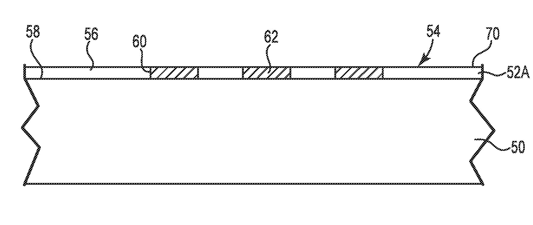
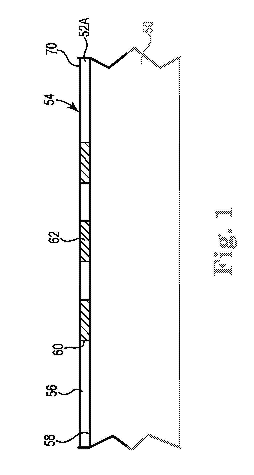
[0038]FIG. 1 is a side sectional view of substrate 50 with first layer 52A of a compliant printed circuit 54 for making a semiconductor package in accordance with an embodiment of the present disclosure. In the preferred embodiment, the first layer 52A includes dielectric material 56 selectively printed on surface 58 of the substrate 50.

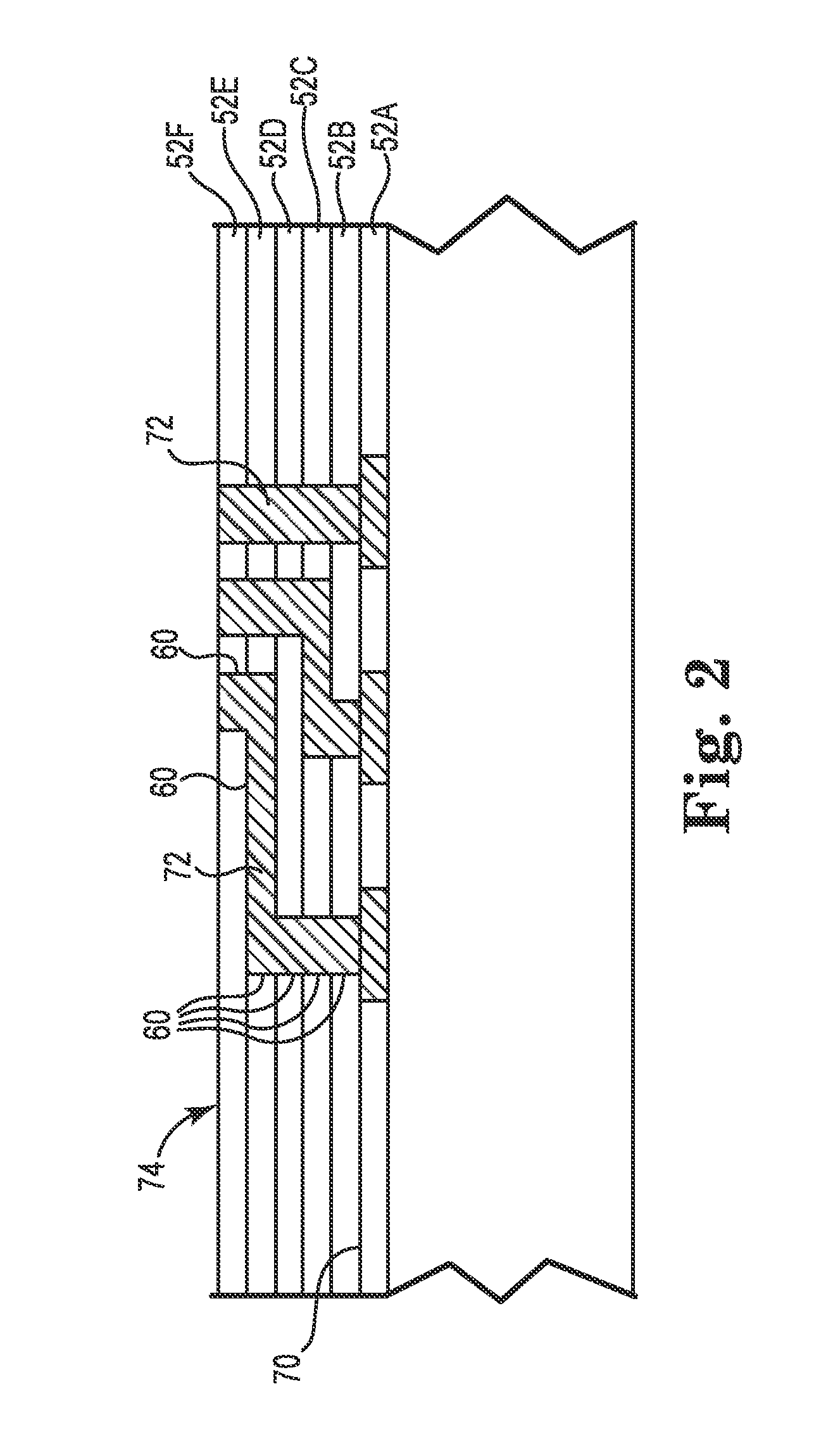
[0039]Recesses 60 in the dielectric material 56 are then metalized to create contact members 62. Metalizing can be performed by printing conductive particles followed by a sintering step, by printing conductive inks, or a variety of other techniques. The metalizing material is preferably of copper or similar metallic materials such as phosphor bronze or beryllium-copper. The resulting contact members 62 are optionally plated to improve conductive properties. The plating is preferably a corrosion resistant metallic material such as nickel, gold, silver, palladium, or multiple layers thereof. FIG. 2 illustrates additional printed layers 52B, 52C, 52D, ...


PUM

PropertyMeasurementUnit
aspect ratioaaaaaaaaaa

Abstract

A compliant printed circuit semiconductor package including a compliant printed circuit with at least a first dielectric layer selectively printed on a substrate with first recesses. A conductive material is printed in the first recesses to form contact members accessible along a first surface of the compliant printed circuit. At least one semiconductor device is located proximate the first surface of the compliant printed circuit. Wirebonds electrically couple terminals on the semiconductor device to the contact members. Overmolding material seals the semiconductor device and the wirebonds to the first surface of the compliant printed circuit. Contact pads on a second surface of the compliant printed circuit are electrically coupled to the contact members.

Description

TECHNICAL FIELD[0001]The present disclosure leverages the capabilities of the additive printing process to create a no lead IC package that has internal compliance near the terminals that are soldered to the PCB. The printing process provides unique opportunity to add function or performance enhancement within the package structure not seen in traditional packages.BACKGROUND OF THE INVENTION[0002]Traditional semiconductors and IC devices are typically packaged in a variety of ways to provide redistribution from the terminals on the die to a spacing that is conducive to cost effective printed circuit board (“PCB”) fabrication techniques. In many cases, the size and distance between die terminals is so small that the device cannot be connected to the final PCB without some sort of fan out or routing. The packages also serve to protect the fragile silicon or provide additional functions such as thermal management or near device decoupling. In many cases, the size and distance between d...

Claims


Application Information

Patent Timeline
Patent Type & Authority Applications(United States)
IPC IPC(8): H05K1/16H05K3/30
CPCH01L21/4867Y10T29/49146H01L23/49822H01L23/4985H01L24/48H01L25/0655H01L2221/68345H01L2224/48091H01L2224/48235H01L2225/0651H01L2924/01004H01L2924/01046H01L2924/01078H01L2924/01079H01L2924/09701H01L2924/12044H01L2924/14H01L2924/15174H01L2924/19041H01L2924/19042H01L2924/19043H01L2924/3011H01L2924/3025H05K3/4664H05K3/4682H01L21/6835H01L2924/30107H01L2224/73265H01L2224/48227H01L2224/32225H01L2924/00014H01L2924/00012H01L2924/00H01L24/73H01L2924/181Y10T29/4913Y10T29/49155
Inventor RATHBURN, JAMES
Owner HSIO TECH
Why Eureka
Try Eureka