
Microelectronic assemblies with cavities, and methods of fabrication

a technology of microelectronic assemblies and cavities, applied in the direction of semiconductor devices, semiconductor/solid-state device details, electrical apparatus, etc., can solve the problems of cracking or detachment of connections, failure of microelectronic assemblies, and difficulty in connecting assemblies to other circuits

Active Publication Date: 2016-10-25
INVENSAS CORP
View PDF156 Cites 52 Cited by
  • Summary
  • Abstract
  • Description
  • Claims
  • Application Information

AI Technical Summary

Benefits of technology

The present invention provides manufacturing processes for multichip modules. One feature is that the lid is attached before underfill deposition, which means the lid is attached before the module fabrication is completed. This helps to prevent any issues that might occur during the attachment process. Another feature is that the lid is made using semiconductor material with a CTE that matches the module or at least one of its components (e.g. an interposer). These technical features improve the manufacturing process for multichip modules.

Problems solved by technology

A common source of failure in microelectronic assemblies is cracking or detachment of connections 124 due to thermal stresses, i.e. mechanical stresses caused by thermal expansion and contraction that may occur during manufacture and subsequent use (operation) of the assembly.
Therefore, when the assembly is heated, the WS expands more than the die, pulling the connections 124 sideways and causing damage.
Further, such thermal stresses may warp the assembly and make it harder to connect the assembly to other circuits.
However, a typical underfill is based on organic polymers which themselves have high CTEs and thus tend to increase the warpage.
This pressure may break the assembly, and even if the assembly is not broken the assembly remains stressed, and this residual stress may break the assembly later on, especially when additional stresses are introduced by subsequent fabrication steps or during operation.

Method used


Image

  • Microelectronic assemblies with cavities, and methods of fabrication
  • Microelectronic assemblies with cavities, and methods of fabrication
  • Microelectronic assemblies with cavities, and methods of fabrication

Examples


Embodiment Construction

[0023]The embodiments described in this section illustrate but do not limit the invention. The invention is defined by the appended claims.

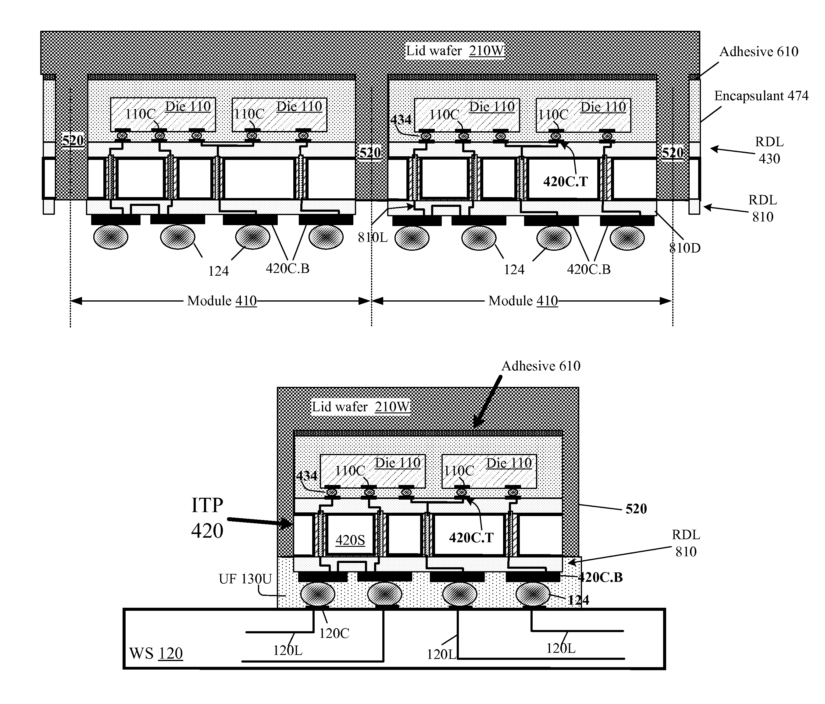
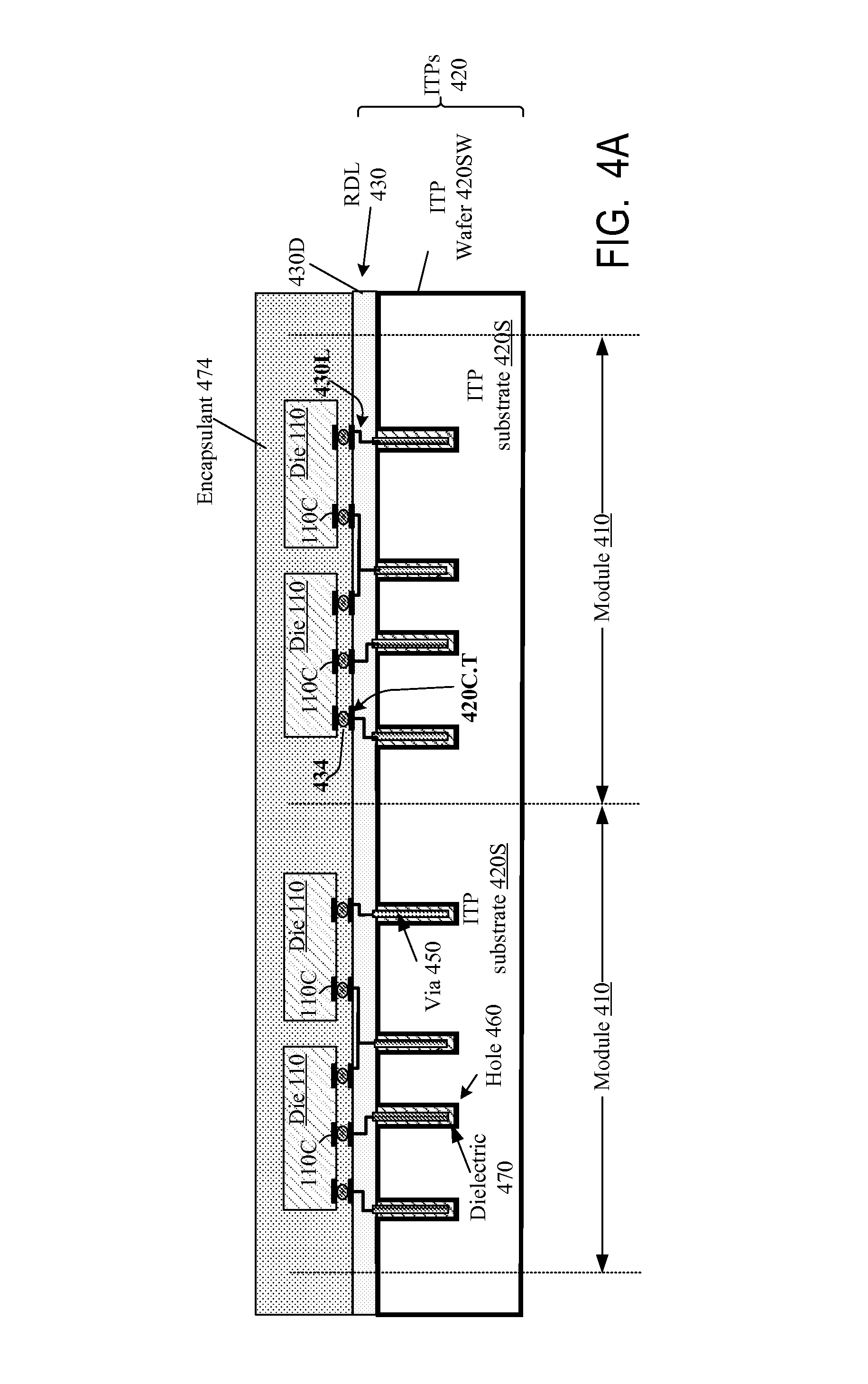
[0024]FIG. 4A illustrates early stages of fabrication of multichip modules 410 which of which contains a stack of die that will be capped by a lid according to some embodiments of the present invention. For illustration purposes, the figure shows multiple modules 410 fabricated in batch and later separated from each other. Modules 410 may have many different architectures, and for the sake of illustration each module 410 contains a stack of an interposer die 420 with two die 110 on top. Each interposer (ITP) 420 will have bottom contact pads attachable to other components, e.g. WS 120 of FIG. 1; these contact pads have not yet been formed. Thus, the die 110 will be connected to the WS or other components through the interposer rather than directly. The interposer can be used for various reasons. One reason is that sometimes the WS contact pads 12...


PUM


Abstract

Die (110) are attached to an interposer (420), and the interposer / die assembly is placed into a lid cavity (510). The lid (210) is attached to the top of the assembly, possibly to the encapsulant (474) at the top. The lid's legs (520) surround the cavity and extend down below the top surface of the interposer's substrate (420S), possibly to the level of the bottom surface of the substrate or lower. The legs (520) may or may not be attached to the interposer / die assembly. In fabrication, the interposer wafer (420SW) has trenches (478) which receive the lid's legs during the lid placement. The interposer wafer is later thinned to remove the interposer wafer portion below the legs and to dice the interposer wafer. The thinning process also exposes, on the bottom, conductive vias (450) passing through the interposer substrate. Other features are also provided.

Description

BACKGROUND OF THE INVENTION[0001]The present invention relates to microelectronic assemblies and to methods for manufacturing such assemblies. Some embodiments provide reliable assemblies and simplify some aspects of the manufacturing process.[0002]FIG. 1 illustrates a typical microelectronic assembly in which a semiconductor die 110 is attached to a wiring substrate (WS, e.g. printed circuit board) 120. The die was manufactured as part of a semiconductor wafer in a single process with other die, and was then separated from the wafer. The die's contact pads 110C are attached to contact pads 120C of WS 120. The attachments 124 can be solder for example. WS 120 has conductive lines 120L used to connect the die to other circuitry (not shown).[0003]A common source of failure in microelectronic assemblies is cracking or detachment of connections 124 due to thermal stresses, i.e. mechanical stresses caused by thermal expansion and contraction that may occur during manufacture and subseque...

Claims


Application Information

Patent Timeline
IPC IPC(8): H01L21/44H01L23/00H01L23/498H01L23/31H01L23/053H01L25/065H01L21/48
CPCH01L23/562H01L21/4853H01L21/486H01L21/481H01L23/49838H01L23/49827H01L23/3114H01L23/053H01L25/0655H01L24/97H01L23/295H01L21/561H01L24/13H01L24/16H01L24/32H01L24/48H01L24/73H01L24/92H01L2224/0401H01L2224/04042H01L2224/13111H01L2224/16227H01L2224/32225H01L2224/32245H01L2224/48227H01L2224/73204H01L2224/73253H01L2224/92225H01L2224/97H01L2924/10253H01L2924/15192H01L2924/15311H01L2924/157H01L2924/15788H01L2924/16153H01L2924/16235H01L2924/16251H01L2924/16315H01L2924/167H01L2924/16787H01L2924/16788H01L2924/3511H01L2924/1632H01L23/145H01L23/147H01L23/15H01L23/3675H01L23/5384H01L23/3128H01L2924/00014H01L21/76898H01L2224/81H01L2224/85H01L2224/83H01L2924/01029H01L2224/45015H01L2924/207H01L2224/45099H01L2224/16225H01L2924/00
Inventor SHEN, HONGWANG, LIANGKATKAR, RAJESHWOYCHIK, CHARLES G.GAO, GUILIAN
Owner INVENSAS CORP
Features
  • Generate Ideas
  • Intellectual Property
  • Life Sciences
  • Materials
  • Tech Scout
  • Unparalleled Data Quality
  • Higher Quality Content
  • 60% Fewer Hallucinations
Learn More