Photonic-crystal slab absorber and high-frequency circuit and electronic components, and transmitter, receiver and proximity wireless communication system

a technology of photonic crystal and high-frequency circuit, which is applied in the field of photonic crystal (pc) slab absorber, high-frequency circuit, electronic component, transmitter, receiver, etc., can solve the problems of large-scale and expensive configurations required for such thz-wave systems, difficult to produce hollow metal waveguides used in the electric wave region, and difficult integration. , to achieve the effect of high absorption and absorption effect, easy processing, and high absorption and absorption bandwidth

Active Publication Date: 2016-11-15
ROHM CO LTD +1
View PDF10 Cites 0 Cited by
  • Summary
  • Abstract
  • Description
  • Claims
  • Application Information

AI Technical Summary

Benefits of technology

[0024]According to the present invention, there can be provided the thin and flat type PC slab absorber having high capturing and absorption effects and the easy processability, and the high-frequency circuit, the electronic component to which such a PC slab absorber is applied.
[0025]Moreover, according to the present invention, there can be provided the PC slab absorber which can increase the absorptivity and absorption bandwidth by introducing the reflecting mirror into the PC slab absorber, and adjusting the distance between the reflecting mirror and the photonic crystal.
[0026]Moreover, according to the present invention, there can be provided the transmitter, the receiver, and the proximity wireless communication system to which the PC slab absorber which introduces the reflecting mirror is applied.

Problems solved by technology

However, since THz-wave systems are composed of large-sized and three-dimensional structured components under the current circumstances, large-sized and expensive configurations are required for such THz-wave systems.
However, optical components, e.g. lenses, mirrors, are composed of large-sized and three-dimensional structured components, and therefore are not suitable for the integration.
Moreover, it is becoming difficult to produce hollow metal waveguides used in the electric wave region due to its fine three-dimensional structure.
Furthermore, a waveguide loss in planar metallic-transmission lines is increased as effect of metallic absorption is increased.

Method used


Image

  • Photonic-crystal slab absorber and high-frequency circuit and electronic components, and transmitter, receiver and proximity wireless communication system
  • Photonic-crystal slab absorber and high-frequency circuit and electronic components, and transmitter, receiver and proximity wireless communication system
  • Photonic-crystal slab absorber and high-frequency circuit and electronic components, and transmitter, receiver and proximity wireless communication system

Examples


first embodiment

[First Embodiment]

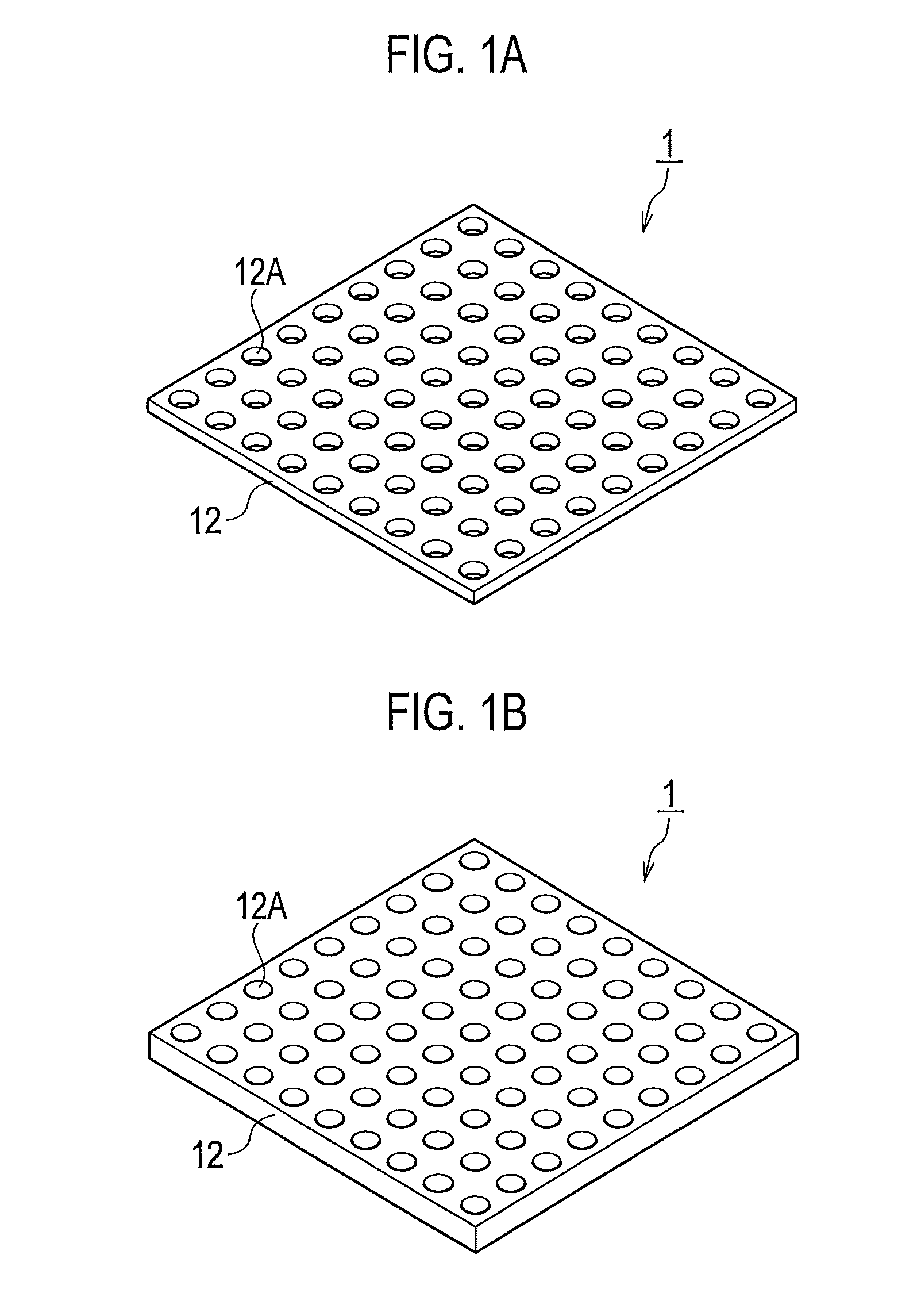
[0131]FIG. 1A shows a schematic bird's-eye view structure of a PC slab absorber 1 according to a first embodiment, and FIG. 1B shows another schematic bird's-eye view structure.

[0132]As shown in FIGS. 1A and 1B, the PC slab absorber 1 according to the first embodiment includes: a 2D-PC slab 12 composed of semiconducting materials; and a lattice point 12A periodically arranged in the 2D-PC slab 12, the lattice point for forming resonant-state (resonant-state-forming lattice) 12A which can capture an electromagnetic wave incident from an outside by resonating an electromagnetic wave in a band edge of a photonic band structure of the 2D-PC slab 12 in the plane of the 2D-PC slab 12. In this case, the 2D-PC slab 12 is doped with impurities and can absorb the captured electromagnetic wave in the band edge resonant frequency.

[0133]In the PC slab absorber according 1 to the first embodiment, as shown in FIG. 1A, the lattice point for forming resonant-state 12A may include ...

second embodiment

[Second Embodiment]

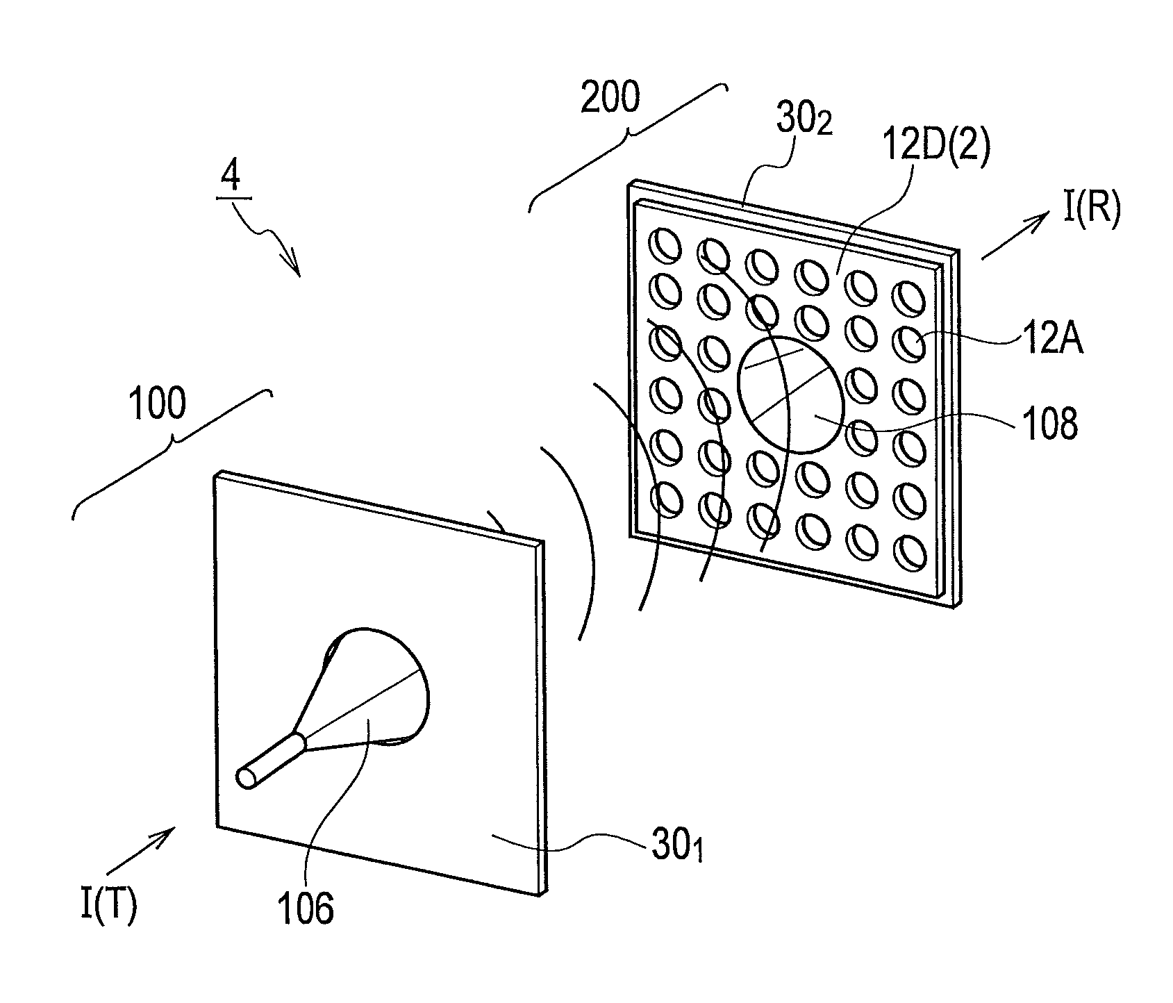
[0263]FIG. 49 shows a PC slab absorber according to a second embodiment, and shows in particular a schematic diagram illustrating the capturing and absorption effects in the PC slab absorber 3 in which a reflecting mirror 30 is introduced to a back side of the 2D-PC slab 12D.

[0264]As shown in FIG. 49, also in the PC slab absorber 3 according to the second embodiment, the incident electromagnetic wave II is resonated and captured in the plane of the 2D-PC slab 12D, in the same manner as the first embodiment. Moreover, the incident electromagnetic wave II is absorbed with materials of the 2D-PC slab 12D. More specifically, the PC slab absorber 3 according to the second embodiment also can increase the absorptive ability due to the synergistic effect between the capturing and the absorption (capturing+absorption).

[0265]Furthermore, the PC slab absorber 3 according to the second embodiment reflects the transmitted electromagnetic wave IT by introducing the reflecting ...

experiment 1

(Result of Spectrogram)

[0281]FIG. 53A shows a comparison of spectrograms of the THz TDS observing simultaneously between the capturing effect (time domain) and the band edge effect (frequency domain), in the PC slab absorber according to the second embodiment, and shows in particular an example of a high resistivity slab without the PC and without the absorption. FIG. 53B shows in particular an example of a high resistivity slab with the PC and without the absorption. FIG. 53C shows in particular an example of a high resistivity slab with the PC slab and the reflecting mirror, and without the absorption. FIG. 53D shows in particular an example of a low resistance slab without the PC and with the absorption. FIG. 53E shows in particular an example of a low resistance slab with the PC and with the absorption. FIG. 53F shows in particular an example of a low resistance slab with the PC slab and the reflecting mirror, and with the absorption.

[0282]In the present embodiment, the period ...


PUM


Abstract

The photonic-crystal (PC) slab absorber includes: a two-dimensional (2D)-PC slab composed of semiconducting materials; and a lattice point periodically arranged in the 2D-PC slab, the lattice point for forming resonant-state which can capture an electromagnetic waves incident from an outside by resonating an electromagnetic wave in a band edge of a photonic band structure of the 2D-PC slab in the plane of the 2D-PC slab. The 2D-PC slab is doped with impurities and can absorb the captured electromagnetic wave in the band edge resonant frequency of the 2D-PC slab.

Description

CROSS REFERENCE TO RELATED APPLICATIONS AND INCORPORATION BY REFERENCE[0001]This application is based upon and claims the benefit of priority from prior Japanese Patent Application Nos. P2013-46780 filed on Mar. 8, 2013, and P2014-28821 filed on Feb. 18, 2014, the entire contents of which are incorporated herein by reference.TECHNICAL FIELD[0002]The present invention relates to a photonic-crystal (PC) slab absorber, a high-frequency circuit, an electronic component, a transmitter, a receiver, and a proximity wireless communication system. In particular, the present invention relates to a thin and flat type PC slab absorber having high capturing and absorption effects and an easy processability, and a high-frequency circuit, an electronic component, and a transmitter, receiver, and a proximity wireless communication system to which such a PC slab absorber is applied.BACKGROUND ART[0003]In recent years, for THz wave band (0.1 THz to 10 THz) positioned in intermediate frequencies betwe...

Claims


Application Information

Patent Timeline
Patent Type & Authority Patents(United States)
IPC IPC(8): G02B1/02H01Q17/00G02B1/00G02B5/00B82Y20/00G02B6/122H01Q15/00
CPCH01Q17/00B82Y20/00G02B1/005G02B5/003G02B6/1225H01Q15/006
Inventor FUJITA, MASAYUKINAGATSUMA, TADAOKAKIMI, RYOMAONISHI, DAIMIYAI, EIJI
Owner ROHM CO LTD
Why Eureka
Try Eureka